Silicon Photonics Wafer-Level Test Equipment Market Analysis (2027 - 2033)
This Report Provides In-Depth Analysis of the Silicon Photonics Wafer-Level Test Equipment Market Report Prepared by P&S Intelligence, Segmented by Equipment Type (Wafer Probe Systems, Optical Probe Cards and Optical Interface Assemblies, Optical Test and Measurement Instruments, ATE Platforms, Test Software), Test Configuration (Single-Sided Wafer-Level Test, Double-Sided Opto-Electronic Wafer Test), Automation Level (Fully Automatic, Semi-Automatic), Wafer Size (300 mm, 200 mm, 150 mm and Below), Application (Data Center and HPC, Telecommunications, Automotive LiDAR and Sensing, Healthcare and Biosensing), and Geographical Outlook for the Period of 2022 to 2033
Silicon Photonics Wafer-Level Test Equipment Market Statistics
Key Highlights
Study Period
2022 - 2033
Market Size in 2026
USD 442.63 Million
Market Size in 2027
USD 496.41 Million
Market Size by 2033
USD 987.73 Million
Projected CAGR
12.15%
Largest Region
Asia-Pacific
Fastest Growing Region
Asia-Pacific
Market Structure
Moderately Fragmented
Market Size
Explore the market potential with our data-driven report
Silicon Photonics Wafer-Level Test Equipment Market Overview
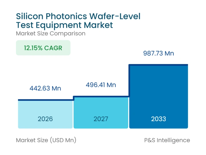
The global silicon photonics wafer-level test equipment market size is estimated at USD 442.63 million in 2026 and is projected to reach USD 496.41 million in 2027. Revenue is projected to climb to USD 987.73 million by 2033, advancing at a CAGR of 12.15% during 2027-2033. Foundries, IDMs, and OSATs ramping optical engines for AI clusters are buying photonic probe systems and opto-electronic test cells so that faulty photonic dies are rejected before expensive bonding and packaging steps begin.
AI cluster builders moving to co-packaged optics are a leading source of new test-cell orders, because an optical engine sealed beside a switch ASIC or GPU cannot be reworked once a faulty photonic die is inside. NVIDIA said in March 2025 that its Spectrum-X Photonics Ethernet switches would reach the market in 2026 through infrastructure and system vendors. Switch launches of this kind size the platform base, not test equipment adoption, but they raise the cost of a missed defect for every foundry supplying the engines. That raises the value of wafer-level known-good-die screening for every engine program.
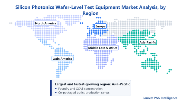
Asia-Pacific accounts for more than half of 2026 revenue and is also the fastest-expanding region, with a 13.6% CAGR forecast for 2027-2033. Taiwan's foundries and OSATs, China's optical module makers, and Singapore's silicon photonics foundries install test cells beside the wafer output they screen, so each new production line in these countries brings capacity-led orders. North America ranks second, and its silicon photonics wafer-level test equipment demand leans more on upgrades at design houses, accelerator developers, and U.S. fabs that already operate photonic probe stations.
Key market insights
By equipment type, optical probe cards and optical interface assemblies hold 25.4% in 2026, while ATE platforms are set to expand at a 14.8% CAGR during 2027-2033.
By test configuration, single-sided wafer-level test holds the larger share in 2026, while double-sided opto-electronic wafer test is expected to post a 15.6% CAGR during 2027-2033.
By automation level, fully automatic holds 52.4% in 2026 and is also forecast to grow fastest, at a 13.2% CAGR during 2027-2033.
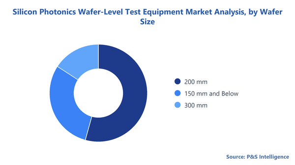
By wafer size, 200 mm holds 54.3% in 2026, while 300 mm is projected to advance at a 16.8% CAGR during 2027-2033.
By application, data center and HPC holds 32% in 2026 and is also expected to grow fastest, at a 14.9% CAGR during 2027-2033.
By geography, Asia-Pacific holds 52% in 2026 and is also projected to record the fastest growth, at a 13.6% CAGR during 2027-2033.
Silicon Photonics Wafer-Level Test Equipment Market Drivers & Opportunities
Co-packaged optics ramps are driving known-good-die screening onto the photonic wafer
Co-packaged optics changes the price of a missed defect, and that change helps explain why foundries and OSATs are adding wafer-level photonic test capacity. Once an optical engine shares a package with a switch ASIC or GPU, one faulty photonic die can scrap a costly multi-chip assembly instead of a single pluggable module. Fabs respond by buying probe systems, optical interface assemblies, and opto-electronic testers that sort photonic and electronic dies before bonding, which moves test spending upstream in the production flow.
TSMC has stated that a co-packaged optics solution using its COUPE engine on substrate begins production in 2026, with the engine stacking an electrical die on top of a photonic die. A production start of this kind sets the volume of bonded wafers that need screening, although it does not fix how many test cells each fab will buy. Test vendors able to handle stacked electronic-photonic wafers at production throughput are better positioned for early volume orders, since fabs tend to qualify one test flow and then repeat it across lines.
Double-sided probing of bonded wafers is redefining test cell design
Hybrid bonding of electronic and photonic wafers is changing what a wafer-level test cell must do. When the electrical die sits above the photonic layer, electrical probes contact the wafer from the top while optical coupling happens from the bottom, so a conventional single-sided prober cannot test the bonded stack. Fabs adopting this architecture need new chucks, optical alignment from below, and testers that coordinate both access paths, which is likely to raise the equipment value of each cell compared with single-sided setups.
Teradyne described the cell it introduced with ficonTEC in March 2025 as the first high-volume double-sided wafer probe test system for silicon photonics, pairing UltraFLEXplus ATE with ficonTEC optical alignment, probing, and wafer handling for hybrid-bonded PIC and EIC wafers. The same release presents the cell as fitting existing fab and OSAT test floors. For ATE vendors, the architecture brings photonic sort onto testers that fabs already run for electrical sort, so photonic test spending can grow inside installed tester fleets instead of on a separate optical platform.
Shared photonic pilot lines are opening a new tier of test equipment buyers
Startups, universities, and smaller fabless photonics firms rarely justify a dedicated wafer-level test cell, yet they need measured wafer data to win design-ins with module makers. Publicly funded pilot lines that run multi-project wafers with packaging and test services pool that demand, and each site adding a test service line needs probe stations, optical instruments, and analysis software. Orders from these sites are smaller than foundry orders and are likely to favor flexible semi-automatic stations that handle many device types.
Per imec, the European PIXEurope pilot line brings together 20 institutions from 11 countries and covers the chain from design and fabrication through integration, packaging, and testing. Users are scheduled to gain access to existing partner sites from November 2026, with new pilot-line infrastructure due from May 2027 and full operational capacity expected by May 2028. A staged schedule like this suggests equipment purchases spread across 2027 and 2028, giving probe-system and instrument vendors a visible pipeline of research-grade orders outside the hyperscale supply chain.
Slow optical alignment and high test cost are limiting test coverage per wafer
Optical test runs far slower than electrical sort because each device needs fiber or probe alignment to sub-micron tolerances before a measurement starts. That bottleneck can push fabs to sample a subset of dies per wafer or skip some optical parameters, which can reduce the number of test cells bought per wafer start and delays full-coverage test until throughput improves. Test methods also differ between foundries and customer programs, so each new program defines its own flow and qualification takes longer.
Fraunhofer IZM, describing the PhotonicLEAP Horizon 2020 project in 2021, put packaging and testing at over 75% of total PIC manufacturing cost. A cost share that large makes test a direct target for savings, giving buyers reason to press on price per tested die and time per wafer. Equipment makers are answering with parallel alignment engines and multi-channel optical probing, but until those designs reach production throughput, test budgets at some fabs are likely to grow more slowly than wafer output.
Segmentation Analysis
Equipment Type
Optical probe cards and optical interface assemblies account for 25.4% of silicon photonics wafer-level test equipment market revenue in 2026, the largest share by equipment type. Each card or interface is built around a specific coupler layout and pad map, so a new photonic design or foundry process usually brings a new assembly order even when the prober stays in place. According to Jenoptik's product page, its UFO Probe Card runs parallel optical and electronic tests on wafers using standard IC probers and ATE, which lets fabs add optical sort without buying a new prober.
ATE platforms are projected to post the fastest growth, at a 14.8% CAGR during 2027-2033. Testers and optical instruments are counted here only when configured or sold for silicon photonics wafer test, and revenue from general electrical automated test equipment is excluded. Growth is likely to come from co-packaged optics programs that sort the electronic and photonic layers of one bonded wafer in a single insertion, moving photonic test onto production testers that fabs already operate. ATE vendors with photonic instrument options are therefore better positioned to sell into installed tester fleets.
Test Configuration
Single-sided wafer-level test holds the larger share of 2026 revenue in the configuration split. Many silicon photonic wafers in production expose both optical couplers and electrical pads on the top surface, so fabs can use conventional probe stations fitted with fiber alignment and add optical instruments around them. Transceiver photonic integrated circuits for pluggable modules are typically tested this way, and the method suits 200 mm lines whose probers were first bought for electrical sort. Tool vendors here compete mainly on alignment speed and repeatability.
Double-sided opto-electronic wafer test is expected to grow fastest, at a 15.6% CAGR during 2027-2033. Hybrid bonding places the electronic die over the photonic die, so electrical probes land on the top while light couples from beneath, and only purpose-built cells can reach both at once. Each co-packaged optics line that adopts bonded wafers needs this capability from its first production lot. Test-flow qualification therefore becomes an early purchasing decision for these lines, and cell suppliers that clear the first qualification are better positioned for the follow-on capacity orders at the same fab.
Automation Level
Fully automatic systems account for 52.4% of 2026 revenue and lead the automation split. Production fabs need wafer loading, fiber alignment, measurement, and data transfer to run without an operator, because manual alignment cannot keep pace with wafer starts for transceiver and optical engine programs. Keysight lists SECS/GEM factory automation and clean-room-ready features on the page for its NX5402A silicon photonics wafer test system, the kind of integration fabs expect before a tool joins a high-volume line.
Fully automatic systems are also projected to grow fastest, at a 13.2% CAGR during 2027-2033. Foundries moving co-packaged optics from lab qualification into volume production are likely to add cassette-fed systems that run multi-site wafer maps unattended, alongside the semi-automatic stations they use for characterization. Semi-automatic stations remain the usual tool for design houses and research labs, so their demand tracks new design starts and pilot-line budgets more closely than wafer volume. For vendors, this splits the order book between production fleets and lab tools.
Wafer Size
200 mm wafers account for 54.3% of 2026 revenue. Many silicon photonics foundry processes were built on 200 mm lines with depreciated equipment and mature process design kits, so much of today's transceiver PIC volume still comes from these wafers. Test cells sized for 200 mm are also common at design houses and labs that evaluate prototypes before a design moves into production, which keeps 200 mm probe stations in steady demand across both production and development buyers.
300 mm wafers are projected to grow fastest, at a 16.8% CAGR during 2027-2033. Foundries building co-packaged optics engines run photonic and electronic processes on 300 mm lines, and bonded wafer stacks need test chucks and handling matched to that diameter. EXFO's OPAL-EC page shows a stage that holds wafers up to 12 inches (300 mm) and offers multiport edge-coupling tests at wafer level, an example of probe stations adapting to the larger format. The shift raises the weight of 300 mm-capable chucks and handlers in new orders.
Copyright P&S Intelligence. Reuse requires attribution under CC BY 4.0.
Application
Data center and HPC applications hold 32% of 2026 revenue, the largest application share. Optical transceivers and co-packaged optics engines for AI clusters account for a large portion of silicon photonic wafer starts at high-volume foundries, and these devices pass through electrical and optical sort before dicing. FormFactor's annual report for fiscal 2025 states that the company is working with certain customers to move co-packaged optics from the lab to the fab, a sign that test equipment buyers are preparing production capacity for this application.
Data center and HPC is also set to expand fastest, at a 14.9% CAGR during 2027-2033. Each step to a faster lane rate, such as the move from 800G to 1.6T optics, brings new PIC designs, new probe cards, and new test recipes, so equipment spending follows design turns as well as wafer volume. Telecommunications, automotive LiDAR, and biosensing programs use the same tool types, which lets equipment vendors spread development costs across several end markets.
The following segments are analysed in this report.
Equipment Type
Wafer Probe Systems
Optical Probe Cards and Optical Interface Assemblies
Optical Test and Measurement Instruments
ATE Platforms
Test Software
Test Configuration
Single-Sided Wafer-Level Test
Double-Sided Opto-Electronic Wafer Test
Automation Level
Fully Automatic
Semi-Automatic
Wafer Size
300 mm
200 mm
150 mm and Below
Application
Data Center and HPC
Telecommunications
Automotive LiDAR and Sensing
Healthcare and Biosensing
Others
Copyright P&S Intelligence. Reuse requires attribution under CC BY 4.0.
Geographical Analysis
Asia-Pacific silicon photonics wafer-level test equipment market outlook
Asia-Pacific holds 52% of the silicon photonics wafer-level test equipment market in 2026 and is also set to expand fastest, at a 13.6% CAGR during 2027-2033. The region combines much of the world's silicon photonics foundry and OSAT capacity with the module makers that buy finished PICs, so test cells sit on the same campuses as the wafers they screen. China is the region's largest market and also its fastest-growing country, with demand tied to domestic optical module makers sourcing PICs at volume for 800G and 1.6T products.
Taiwan is central to the region's co-packaged optics buildout. As per SEMI, its Taiwan-based Silicon Photonics Industry Alliance brings together over 110 companies, and one of the alliance's three special interest groups covers advanced packaging and testing for co-packaged optics. A shared working group on test suggests local foundries, OSATs, and toolmakers aim to settle common test flows before volume ramps. Singapore adds 200 mm silicon photonics foundry capacity, while Japan and South Korea contribute instrument makers and packaging lines, and the region's share is likely to rise as bonded-wafer lines begin volume output.
Copyright P&S Intelligence. Reuse requires attribution under CC BY 4.0.
North America market analysis
North America trails Asia-Pacific in revenue but generates much of the design and system demand that sets test requirements. Silicon photonics design activity in the U.S. and Canada, spanning AI accelerator and switch developers and fabless photonics firms, creates lab demand for characterization and qualification, while volume wafer sort for many of these parts takes place at Asian foundries. Regional demand therefore leans toward high-specification, flexible systems and instrument upgrades with each new lane rate. Design teams often match their foundry partners' instrument families so lab and fab data correlate, tying lab purchases to suppliers already qualified at the fab.
Domestic production capacity could add volume buyers over the forecast period. GlobalFoundries announced in July 2026 a letter of intent under which the U.S. Department of Commerce's CHIPS R&D Office is expected to award it USD 300 million for optical materials, wafer technologies, and advanced packaging, including 3D hybrid bonding for co-packaged optics, at sites in Malta, New York, and Burlington, Vermont. If the award is finalized, the program would add U.S. demand for bonded-wafer test capability, where local ATE and probe-system suppliers already hold application expertise.
Europe market analysis
Europe holds a smaller share than the two leading regions, with demand concentrated in research institutes, pilot lines, and specialty fabs instead of high-volume transceiver production. Public research fabs in Germany and France run multi-project silicon photonics wafers for startups and universities, and the Netherlands hosts integrated photonics programs with similar needs. Because each multi-project wafer carries many unrelated designs, these sites value flexible test recipes and fast probe changes over raw throughput, which favors semi-automatic probe stations and general-purpose optical instruments. University photonics research in the U.K. uses similar lab-scale tools for device work.
Germany also supplies equipment to the wider market, since precision alignment specialists and ficonTEC's photonic assembly and test business are based there, which keeps engineering contact between toolmakers and European fabs close. European demand is likely to step up as EU-funded pilot-line infrastructure comes online and adds test service lines that need wafer-level tools. Vendors with application-engineering staff in these countries could gain repeat research orders as those service lines expand.
Latin America market analysis
Latin America contributes a small share of global revenue, and commercial demand for wafer-level photonic test equipment is minimal because the region has no volume silicon photonics wafer fabs. Any purchases are likely to be research-scale orders linked to university photonics programs in Brazil and Mexico, where probe stations and optical instruments support device studies instead of production sort. Volumes of this kind are irregular and depend on research grant cycles.
Copyright P&S Intelligence. Reuse requires attribution under CC BY 4.0.
Data center construction in Brazil and Mexico consumes finished optical modules made elsewhere, so it raises local optics deployment without creating wafer-level test demand. That pattern is likely to hold until a regional photonic wafer fab or advanced packaging line is established. For equipment vendors, the region is likely to remain a distributor-served market with occasional laboratory sales until such capacity appears.
Middle East & Africa market analysis
Middle East & Africa has the smallest regional base, and Israel is the main center of photonics design work. Israeli chip and networking design teams develop optical interconnect and photonic devices that need characterization and qualification test, while Saudi Arabia and the U.A.E. are expanding AI data center capacity that consumes finished optics instead of wafers. Commercial demand for wafer-level test equipment outside Israel is minimal.
In June 2026, the Israel Innovation Authority and the defense ministry's DDR&D launched a call for proposals, backed by up to USD 48.83 million (ILS 150 million), to set up an advanced integrated photonics R&D infrastructure whose services would run from design and simulation through characterization, testing, and packaging. If a proposal is approved, the infrastructure must begin some partial services within 12 months, which would create a local buyer of wafer-level probe and optical test equipment. Gulf demand is expected to stay centered on deployed optics.
The following geographies are analysed in this report.
Asia-Pacific
China
Taiwan
Japan
South Korea
Singapore
India
Rest of Asia-Pacific
Europe
Germany
U.K.
France
Netherlands
Rest of Europe
Latin America
Brazil
Mexico
Rest of Latin America
Middle East & Africa
Israel
Saudi Arabia
U.A.E.
Rest of Middle East & Africa
North America
U.S.
Canada
Silicon Photonics Wafer-Level Test Equipment Market Competitive Landscape
The silicon photonics wafer-level test equipment market is moderately fragmented, with competition spread across specialist layers and no single supplier covering the full test cell. A production cell combines a prober, optical alignment and interface hardware, optical instruments, an electrical tester, and software, and each layer has its own specialists with separate qualification histories at fabs. Switching costs are high once a fab has correlated a test flow against its process, because a new tool must reproduce coupling-loss and spectral results before it can sort production wafers.
Probe-system makers FormFactor, MPI, and EXFO, together with Innotech's STAr Technologies unit, compete on alignment speed, wafer handling, and coupler support, from grating to edge couplers at wafer level. ATE suppliers Advantest, Teradyne, and Chroma ATE bring photonic sort onto their production tester platforms, often through partnerships with prober and alignment specialists. Keysight supplies optical and electrical instruments with test software, while Robotechnik, through its ficonTEC business, and PI provide precision alignment hardware used in many cells. Tie-ups such as Teradyne with ficonTEC and FormFactor with Advantest show tester and prober vendors pairing capabilities instead of building every layer alone.
The structure is evolving as ATE and probe-system vendors acquire or partner with photonics specialists to offer integrated cells. For buyers, a layered supply base leaves room to mix vendors, but it also adds integration work, since each layer must be correlated with the others before production release. Fabs scaling co-packaged optics are likely to favor pre-integrated cells from a small set of partner groups, which raises the entry bar for new single-layer specialists.
Major Companies in Silicon Photonics Wafer-Level Test Equipment Market:
Keysight Technologies Inc.
FormFactor Inc.
Advantest Corporation
Teradyne Inc.
MPI Corporation
EXFO Inc.
Robotechnik Intelligent Technology Co. Ltd.
Physik Instrumente (PI) SE & Co. KG
Innotech Corporation
Chroma ATE Inc.
Anritsu Corporation
Yokogawa Electric Corporation
SemiProbe Inc.
Silicon Photonics Wafer-Level Test Equipment Market News & Developments
In June 2026, Advantest Corporation announced a partnership with OpenLight, a heterogeneous silicon photonics integration and custom photonic ASIC design company, to develop an end-to-end test solution for high-volume manufacturing of electro-optical devices such as optical engines. The pairing links a production tester supplier with a photonic design platform, which could shorten test development for chips built on that platform.
In March 2026, Teradyne Inc. introduced Photon 100 at OFC 2026 in Los Angeles, an opto-electric automated test platform built on its UltraFLEXplus system that supports single-sided and double-sided wafer test as well as optical engine and co-packaged module insertions. One tester platform across these insertions lets fabs reuse test programs from wafer sort through module test.
In January 2026, Physik Instrumente (PI) SE & Co. KG introduced a miniaturized alignment engine platform for electro-optical wafer-level test that supports parallel operation of multiple alignment engines across a single wafer, aimed at validating electrical and optical functions simultaneously in high-volume production. Parallel alignment targets the serial fiber alignment that limits optical test throughput per wafer.
In December 2025, FormFactor Inc. acquired Keystone Photonics, a developer of optical probing technology for silicon photonics and co-packaged optics wafer testing, to add its optical probing, alignment technology, and software to FormFactor's electrical, thermal, and RF wafer test offerings. The deal brings optical coupling know-how inside a major probe-system supplier as co-packaged optics programs move toward volume production.
Last Updated: October 2026
Frequently Asked Questions About This Report
How big is the silicon photonics wafer-level test equipment market?+
The global silicon photonics wafer-level test equipment market size is estimated at USD 442.63 million in 2026 and is projected to reach USD 496.41 million in 2027.
Which region leads the silicon photonics wafer test equipment market?+
Asia-Pacific holds 52% of the silicon photonics wafer-level test equipment market in 2026 and is also set to expand fastest, at a 13.6% CAGR during 2027-2033.
Why is wafer-level testing important for co-packaged optics?+
Once an optical engine shares a package with a switch ASIC or GPU, one faulty photonic die can scrap a costly multi-chip assembly instead of a single pluggable module.
What is double-sided wafer probe testing for silicon photonics?+
When the electrical die sits above the photonic layer, electrical probes contact the wafer from the top while optical coupling happens from the bottom, so a conventional single-sided prober cannot test the bonded stack.
Which companies make silicon photonics wafer probe systems?+
Probe-system makers FormFactor, MPI, and EXFO, together with Innotech's STAr Technologies unit, compete on alignment speed, wafer handling, and coupler support, from grating to edge couplers at wafer level.
Want a report tailored exactly to your business need?
Leading companies across industries trust us to deliver data-driven insights and innovative solutions for their most critical decisions. From data-driven strategies to actionable insights, we empower the decision-makers who shape industries and define the future. From Fortune 500 companies to innovative startups, we are proud to partner with organisations that drive progress in their industries.
Client Testimonials
Working with P&S Intelligence and their team was an absolute pleasure – their awareness of timelines and commitment to value greatly contributed to our project's success. Eagerly anticipating future collaborations.
McKinsey & Company
India
Unmatched Standards
Our insights into the minutest levels of the markets, including the latest trends and competitive landscape, give you all the answers you need to take your business to new heights
Complete Data Security
We take a cautious approach to protecting your personal and confidential information. Trust is the strongest bond that connects us and our clients, and trust we build by complying with all international and domestic data protection and privacy laws