This Report Provides In-Depth Analysis of the Hybrid Bonding Wafer Equipment Market Report Prepared by P&S Intelligence, Segmented by Bonding Type (Wafer-to-Wafer (W2W) Hybrid Bonding Equipment, Die-to-Wafer (D2W) Hybrid Bonding Equipment), Equipment Type (Hybrid Bonders (Bonding Systems), Inspection, Alignment & Metrology Systems, Surface Preparation, Activation & Cleaning Systems), Application (Logic & High-Performance Computing (AI Accelerators, Chiplets), Memory, CMOS Image Sensors), Automation Level (Fully-Automatic, Semi-Automatic), End User (Foundries, Integrated Device Manufacturers (IDMs), Outsourced Semiconductor Assembly and Test (OSAT) Providers, Research Institutes), and Geographical Outlook for the Period of 2022 to 2033
Explore the market potential with our data-driven report
Hybrid Bonding Wafer Equipment Market Overview
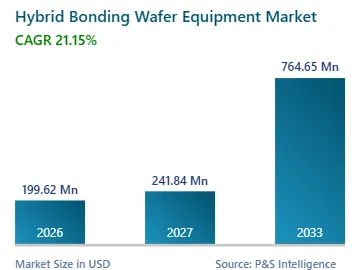
Revenue in the global hybrid bonding wafer equipment market is estimated at USD 199.62 million in 2026 and is projected to rise to USD 241.84 million in 2027. By 2033, sales are projected to reach USD 764.65 million, a CAGR of 21.15% during 2027-2033. New orders come mainly from logic foundries stacking dies for AI accelerators and from memory makers bonding 3D NAND wafers or qualifying the process for high-bandwidth memory. For tool vendors, this puts demand in the hands of a short list of high-volume fabs whose qualification decisions set the timing of orders.
Chipmakers building AI processors are adding bonding and stacking steps to their packaging lines at the same time as their overall tool budgets grow. SEMI data show worldwide semiconductor equipment billings of USD 40.53 billion in the second quarter of 2026, up 23% from a year earlier. That figure covers every front-end and back-end tool, so it measures available capital and not bonder spending. It still matters for hybrid bonding vendors, because bonding lines compete for the same capital approvals as lithography and etch, and a larger pool can make those approvals easier to secure.
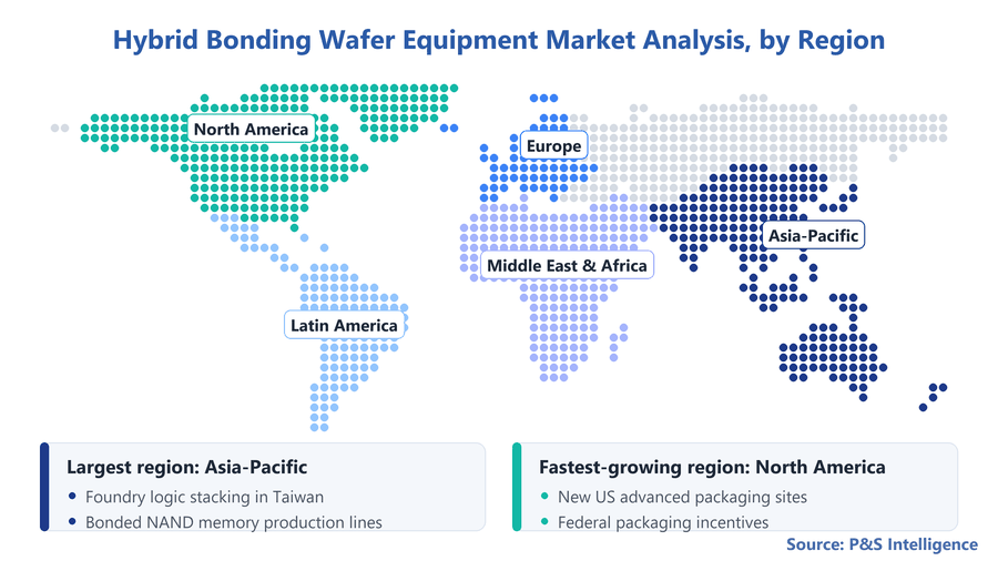
Asia-Pacific accounts for 49% of the hybrid bonding wafer equipment market in 2026, because Taiwan, South Korea, Japan, and China host most of the foundry, memory, image sensor, and 3D NAND lines that buy these tools. North America is projected to post a 21.9% CAGR during 2027-2033, the fastest of any region, as new advanced packaging and memory packaging projects in the U.S. equip lines from a small installed base. Suppliers therefore face two different sales tasks, expanding qualified positions in Asian fabs and competing for first placement at new US sites.
Key market insights
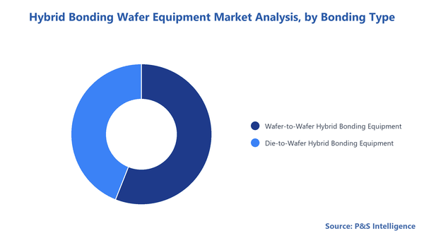
By bonding type, wafer-to-wafer (W2W) hybrid bonding equipment accounts for 56% in 2026, while die-to-wafer (D2W) hybrid bonding equipment is projected to grow the fastest, at a 21.7% CAGR during 2027-2033.
By equipment type, hybrid bonders (bonding systems) account for 43% in 2026, while Inspection, alignment & metrology systems are projected to grow the fastest during 2027-2033.
By application, logic & high-performance computing (AI accelerators, chiplets) accounts for 34% in 2026 and is also the fastest-growing category, with a projected 25.9% CAGR during 2027-2033.
By automation level, fully-automatic systems account for 60% in 2026 and are also projected to grow the fastest during 2027-2033.
By geography, Asia-Pacific accounts for 49% in 2026, while North America is projected to expand at a 21.9% CAGR during 2027-2033.
Integrated bonding platforms are redefining how fabs buy hybrid bonding lines
Chipmakers moving die-to-wafer hybrid bonding into volume production are starting to buy cleaning, surface activation, bonding, and measurement as one connected tool set. Contamination and overlay errors build up while wafers and dies wait between separate machines, so linking the steps cuts queue time and simplifies yield tracking. The purchase then shifts from several vendor contracts per line to a single platform order, with the platform supplier answerable for how the steps work together.
According to Applied Materials, its Kinex system, launched with Besi on October 7, 2025, combines surface preparation, bonding, and metrology in one die-to-wafer tool, aimed at tighter interconnect pitches, consistent bonding quality, and shorter cycle times. For standalone cleaning and inspection specialists, integrated platforms can reduce the number of separate tool orders per line. Buyers, in turn, avoid much of the engineering work of matching tools from different vendors, at the cost of deeper dependence on one supplier for uptime and upgrades.
AI accelerator stacking needs are fueling hybrid bonder orders
Designers of AI accelerators and data center processors want more memory bandwidth and more logic in each package than solder microbumps can connect at acceptable power. Hybrid bonding removes the bump and allows far denser die-to-die links, so a chipmaker that adopts it typically needs added bonding, cleaning, and inspection capacity on its packaging line. A product program that moves to bonded stacks can therefore prompt a capital purchase, usually placed several quarters ahead of volume shipments.
Equipment order books point to this conversion. Besi's half-year results release of July 23, 2026 shows first-half 2026 orders of USD 630.54 million (EUR 562.6 million), up 116.5% from a year earlier, and lists hybrid bonding among the applications behind that strength. That total spans all of Besi's assembly products, of which hybrid bonders are one line. Orders booked in one half-year turn into revenue over later quarters, which can give suppliers holding hybrid bonding backlogs visibility into 2027. Buyers ordering alongside other chip programs may also face longer delivery times for qualified bonders.
Taller high-bandwidth memory stacks are creating a future volume buyer group for bonders
High-bandwidth memory is a large potential buyer group that does not yet buy hybrid bonders in volume. Memory makers stack DRAM dies with thermo-compression bonding today, and each added layer brings bump height and gap that must fit inside a fixed package height. If stack counts and die thinning make bumps impractical, a memory line that converts could need hybrid bonders, cleaning, and inspection tools at production scale, a purchase larger than today's evaluation orders.
StorageNewsletter reported that JEDEC's HBM4 standard (JESD270-4), released April 16, 2025, supports 4-high, 8-high, 12-high, and 16-high DRAM stacks with 24 Gb or 32 Gb die densities. According to SK hynix, existing packaging stays viable through HBM4, with full-scale hybrid bonding more likely from HBM4E or HBM5 as structural limits emerge, and it describes the adoption timing as uncertain given practical constraints. Conversion, when it comes, would favor toolmakers whose bonders have already passed memory makers' evaluations.
Bonding yield risk is constraining the pace of volume adoption
Hybrid bonding leaves no solder to absorb defects, so a particle, a surface step, or a small misalignment can ruin a whole stacked device. In a memory stack of 12 or more dies, a failed interface scraps every known-good die already placed. Chipmakers respond by extending qualification, running pilot lines longer, and keeping proven thermo-compression lines in production until bonded-stack yield approaches that of the incumbent process, which pushes some equipment orders into later years.
Cost adds to the caution. A hybrid bonding line needs front-end-grade surface preparation, chemical mechanical polishing, and post-bond inspection that a bump-based line does not, so the tool bill per unit of capacity tends to be higher. Toolmakers are answering with tighter alignment specifications and integrated platforms that cut handling between steps, though these help yield only once proven in customer lines. The delay mostly affects memory, while image sensor and 3D NAND producers that already bond wafers in volume are less exposed to it.
Segmentation Analysis
bonding Type
Wafer-to-wafer (W2W) hybrid bonding equipment accounts for 56% of hybrid bonding wafer equipment market revenue in 2026. Its lead comes from products that already use bonded wafer pairs in volume. Image sensor makers bond pixel wafers to logic wafers, and some 3D NAND makers build the memory array and its control circuits on separate wafers. In its July 3, 2026 release on 10th-generation BiCS FLASH, Kioxia describes CBA technology, in which CMOS and cell-array wafers are made separately and then bonded together. NAND generations that keep this design turn fab expansions into repeat W2W bonder purchases.
Die-to-wafer (D2W) hybrid bonding equipment is set to post the quickest growth of the two bonding types, a 21.7% CAGR over 2027-2033. D2W lets a chipmaker place only tested, known-good dies onto a target wafer, which matters when dies come from different process nodes or when one bad die would scrap a costly AI processor. Chiplet-based accelerators and future memory stacks both fit this pattern. Most D2W flows place dies in sequence, so a tool processes fewer wafers per hour than a W2W bonder, and a given output needs more systems as programs reach volume.
Copyright P&S Intelligence. Reuse requires attribution under CC BY 4.0.
Equipment Type
Hybrid bonders (bonding systems) account for 43% of revenue in 2026. The bonder is typically the most expensive tool in the line and the one that sets alignment accuracy, so it takes the largest slice of each project budget. Every line needs at least one bonder however the surrounding steps are sourced, and buyers usually qualify the bonder first and fit cleaning and inspection tools around it. Cleaning, activation, inspection, and metrology tools also used in conventional fabs are counted here only when specified for a hybrid bonding process flow.
Inspection, Alignment & Metrology Systems are expected to record the fastest growth. As bond pitches shrink, fabs must measure overlay and detect voids before and after bonding, and they add measurement points as volumes rise. SUSS MicroTec puts the post-bond accuracy of its XBC300 Gen2 D2W platform, introduced in May 2025, at better than ±200 nm, and holding tolerances of that size in production requires measuring bonded wafers routinely. Surface Preparation, Activation & Cleaning Systems grow alongside each new line, while measurement spending rises fastest as alignment specifications tighten.
Application
Logic & high-performance computing (ai accelerators, chiplets) accounts for 34% of revenue in 2026. Foundries that stack cache or compute dies on logic use hybrid bonding to reach interconnect density and power savings microbumps cannot match, and AI processor generations tend to add stacked dies over time. Because each stacked logic wafer carries a high value, buyers accept premium tools and extra inspection to protect yield. Suppliers serving this segment sell into a few foundries whose packaging roadmaps decide when orders arrive.
Logic & high-performance computing revenue is projected to expand at a 25.9% CAGR during 2027-2033, the fastest of the four applications. More chip designers are moving to 3D-stacked chiplets as foundries add bonded stacking to their packaging offers, which spreads demand beyond the first flagship processors. Memory, covering HBM, 3D NAND, and DRAM, would add a second wave if HBM converts to hybrid bonding, while CMOS Image Sensors and MEMS & Others provide steadier, capacity-linked demand. For bonder suppliers, logic programs offer the clearest growth path over the forecast period.
Automation Level
Fully-automatic systems account for 60% of revenue in 2026. Volume lines move wafers in closed carriers from cleaning through bonding to inspection, which keeps particles off bonding surfaces and removes operator handling from the steps most sensitive to contamination. Automatic handling also gives the run-to-run consistency yield engineers need when bonding expensive logic and memory wafers. Production buyers rarely accept manual loading, which confines suppliers without automated handling largely to laboratory sales.
Fully-automatic systems are also expected to grow the fastest, as HBM and chiplet logic programs move from pilot to production and add production-grade tools. Semi-Automatic bonders keep a role in research institutes, university fabs, and early process development, where flexibility and a lower purchase price matter more than throughput. That split leaves semi-automatic suppliers with steady but smaller orders tied to research budgets, while production tool makers capture most of the added volume.
End User
Integrated device manufacturers (IDMs) and Foundries operate the lines where hybrid bonding runs in volume today, because the process needs front-end cleanliness, chemical mechanical polishing, and wafer handling that these fabs already run. Memory IDMs such as SK hynix and Samsung decide HBM bonding adoption inside their own lines, while foundries such as TSMC buy for logic stacking offered to fabless customers. Orders from these two groups tend to arrive in large, program-linked batches.
Outsourced semiconductor assembly and test (OSAT) Providers are a smaller buyer group today, since most assembly sites lack the cleanroom class and polishing steps the process needs. Their role could grow if self-contained die-to-wafer platforms reduce the front-end work an assembly site must run. Research Institutes buy semi-automatic and early production tools for process development and pilot lines, often with public funding, and they serve as reference sites where toolmakers prove new processes before selling to production fabs.
The following segments are analysed in this report:
Bonding Type
Wafer-to-Wafer (W2W) Hybrid Bonding Equipment
Die-to-Wafer (D2W) Hybrid Bonding Equipment
Equipment Type
Hybrid Bonders (Bonding Systems)
Inspection, Alignment & Metrology Systems
Surface Preparation, Activation & Cleaning Systems
Outsourced Semiconductor Assembly and Test (OSAT) Providers
Research Institutes
Geographical Analysis
Asia-Pacific hybrid bonding wafer equipment market outlook
Asia-Pacific accounts for 49% of global revenue in 2026, because the region hosts the production lines where hybrid bonding is already a volume step. Taiwan's foundries stack logic dies for AI processors, South Korea's memory makers are evaluating hybrid bonding for HBM, and Japan and China produce image sensors and 3D NAND built from bonded wafer pairs. Per YMTC, its Xtacking architecture processes periphery circuits and the memory cell array on two separate wafers, then connects them electrically across the whole wafer in one process step.
Taiwan and South Korea are the region's main buying centers, since foundry logic stacking and memory packaging decisions for customers worldwide are made there. Each NAND generation or image sensor expansion that keeps a bonded design brings repeat bonder purchases, an expansion base other regions lack. The lead looks secure through 2033, although the share may ease as US packaging sites come online. For suppliers, local service teams and spare-parts depots weigh heavily when chipmakers choose between vendors that are already qualified.
North America hybrid bonding wafer equipment market growth
North America is projected to post the fastest regional growth, a 21.9% CAGR during 2027-2033. The region starts from a small installed base of hybrid bonding tools, so each new advanced packaging or memory packaging site equips its lines from scratch. Federal incentives have helped bring these projects onshore, and US chip designers building AI processors tend to value packaging capacity close to their product teams. Growth therefore depends on construction schedules, which makes the region's order flow lumpier than Asia-Pacific's.
The U.S. is the region's fastest-growing market. Figures from NIST put SK hynix's CHIPS incentives award at up to USD 458 million, supporting an investment of about USD 3.87 billion in a West Lafayette, Indiana memory packaging plant for AI products and an advanced packaging R&D facility, with funds paid against project milestones. The award does not name a bonding process, so the site marks a potential buyer, not a confirmed hybrid bonding order. Vendors with US installation and field service teams stand to benefit as these sites are equipped.
Copyright P&S Intelligence. Reuse requires attribution under CC BY 4.0.
Europe market analysis
Europe holds a smaller share than the two leading regions, because it lacks high-volume memory and leading-edge logic stacking lines, and public programs fund shared facilities where chip designers and toolmakers test bonded stacks before committing to production. Fraunhofer ENAS lists advancing chip-to-wafer and wafer-to-wafer bonding toward higher integration densities as a key objective of the APECS pilot line, which the Chips Joint Undertaking co-funds with national authorities in eight countries, including Germany, France, and Spain.
Pilot facilities of this kind typically equip with small numbers of development and early production tools, and they act as reference sites where new bonding processes are proven before transfer to fabs elsewhere. Europe is also home to bonding toolmakers in Austria and Germany, which gives local institutes short paths to joint equipment development. European orders are therefore likely to follow pilot-line funding cycles, making them steadier but smaller than the volume orders placed in Asia-Pacific and North America.
Latin America market analysis
Latin America accounts for a small part of global demand, because the region has no volume wafer fabs running hybrid bonding and its semiconductor activity centers on assembly, test, and design. Commercial demand for hybrid bonders is minimal today. Brazil is the clearest policy candidate for future demand. The Chamber of Deputies' news service recorded that Law 14.968, signed in September 2024, extended Padis semiconductor tax incentives from 2026 to 2029 and widened the program's exemptions to include import tax.
Import-tax relief lowers the landed cost of foreign-made tools, which matters in a region where every hybrid bonder would be imported. Mexico's assembly and test sites run conventional packaging, so they are unlikely to need hybrid bonding tools until bonded products move into outsourced assembly. Production orders in the region therefore depend on new front-end investment, which keeps Latin America at the edge of most bonder suppliers' sales plans through the early forecast years.
Middle East & Africa market analysis
The Middle East and Africa contribute a modest share of global revenue, with the region's chip activity concentrated in Israel. Israeli design centers of global processor companies, a specialty foundry, and local metrology and inspection toolmakers give the country a base of 3D integration process work that the rest of the region lacks. Commercial demand for hybrid bonders elsewhere in the region is minimal today, because no volume wafer fab or advanced packaging line there runs the process.
In the United Arab Emirates and Saudi Arabia, semiconductor programs are at an earlier stage, and hybrid bonding purchases would follow only after front-end or advanced packaging capacity is built. Any future Gulf packaging or front-end project would also need imported process know-how alongside the tools, which lengthens the path from announcement to bonder purchase. Until such lines exist, the region adds little to bonder revenue, and suppliers are likely to cover it from sales and support bases in Europe or Asia.
The following geographies are analysed in this report.
Revenue in the hybrid bonding wafer equipment market is concentrated at the bonder layer, where a small group of toolmakers hold systems qualified at the few chipmakers running hybrid bonding in production. Bonding at sub-micrometer overlay calls for alignment and handling know-how built over years, each tool must pass a long qualification inside the customer's line, and the customer base itself is narrow. Cleaning, activation, and inspection steps are more open, because several of those tool types already exist in front-end fabs. The structure is shifting as memory-focused entrants prepare tools for HBM.
Suppliers fall into two main clusters. EV Group and Tokyo Electron sell production wafer-to-wafer bonders into image sensor, 3D NAND, and logic lines, and they compete on overlay accuracy and on how well their bonders work with front-end cleaning and activation. Besi, Applied Materials, SUSS MicroTec, and ASMPT compete in die-to-wafer bonding on placement accuracy, throughput per die, and process integration, with Besi's die-placement technology built into Applied's integrated platform. Because a handful of chipmakers place most production orders, one qualification win or loss can shift a supplier's position for a whole product generation.
Korean equipment makers are opening a third front. Hanwha Semitech completed development of a second-generation hybrid bonder in early 2026, with customer delivery for performance tests planned but not separately confirmed, and Hanmi Semiconductor has announced plans for a hybrid bonder, both aiming at memory makers that already buy their thermo-compression bonders for HBM. For buyers, more qualified sources could widen choice once HBM lines convert. For incumbents, the time and cost of requalifying a running line remain an important protection, since a chipmaker rarely swaps a bonder that already meets its yield targets.
Major Companies in Hybrid Bonding Wafer Equipment Market:
BE Semiconductor Industries N.V.
EV Group Europe & Asia/Pacific GmbH
Applied Materials Inc.
Tokyo Electron Limited
SUSS MicroTec SE
ASMPT Limited
Kulicke and Soffa Industries Inc.
Shibaura Mechatronics Corporation
Canon Inc.
Hanmi Semiconductor Co. Ltd.
Hanwha Semitech Co. Ltd.
Beijing U-Precision Tech Co. Ltd.
Piotech Inc.
Bondtech Co. Ltd.
TAZMO Co. Ltd.
Ayumi Industry Co. Ltd.
SET Corporation SA
Recent Developments in the Market
In May 2026, EV Group Europe & Asia/Pacific GmbH demonstrated wafer-to-wafer hybrid bonding with a research partner at a 200 nm interconnect pitch, with copper pad-to-pad post-bond overlay below 40 nm for every die across a 300 mm wafer, using EV Group’s GEMINI FB system. The result raises the alignment chipmakers can demand when evaluating tools for logic and memory tier stacking.
In February 2026, Hanwha Semitech Co. Ltd. completed development of the SHB2 Nano, its second-generation hybrid bonder, with alignment that holds positioning error to 0.1 micrometer, and planned deliveries to a customer for performance tests in the first half of 2026; a completed delivery has not been separately confirmed. The tool gives South Korean HBM producers another domestic option as they weigh hybrid bonding for taller memory stacks.
In December 2025, BE Semiconductor Industries N.V. placed its first Datacon 8800 CHAMEOultra plus hybrid bonding system into production at a North Carolina advanced packaging customer, delivered earlier in 2025, in what the customer described as the first operational bonder of its kind to do so. The installation gives Besi a US production reference for its newest die-to-wafer bonder.
Last Updated: October 2026
Frequently Asked Questions About This Report
What is the size of the hybrid bonding wafer equipment market?+
Revenue in the global hybrid bonding wafer equipment market is estimated at USD 199.62 million in 2026 and is projected to rise to USD 241.84 million in 2027.
What is driving demand for hybrid bonding equipment?+
Hybrid bonding removes the bump and allows far denser die-to-die links, so a chipmaker that adopts it typically needs added bonding, cleaning, and inspection capacity on its packaging line.
Why does HBM need hybrid bonding?+
Memory makers stack DRAM dies with thermo-compression bonding today, and each added layer brings bump height and gap that must fit inside a fixed package height.
What are the challenges of hybrid bonding?+
Hybrid bonding leaves no solder to absorb defects, so a particle, a surface step, or a small misalignment can ruin a whole stacked device.
What is the advantage of die-to-wafer hybrid bonding over wafer-to-wafer bonding?+
D2W lets a chipmaker place only tested, known-good dies onto a target wafer, which matters when dies come from different process nodes or when one bad die would scrap a costly AI processor.
Which region leads the hybrid bonding equipment market?+
Asia-Pacific accounts for 49% of global revenue in 2026, because the region hosts the production lines where hybrid bonding is already a volume step.
Which companies make wafer-to-wafer hybrid bonding equipment?+
EV Group and Tokyo Electron sell production wafer-to-wafer bonders into image sensor, 3D NAND, and logic lines, and they compete on overlay accuracy and on how well their bonders work with front-end cleaning and activation.
Who makes die-to-wafer hybrid bonding equipment?+
Besi, Applied Materials, SUSS MicroTec, and ASMPT compete in die-to-wafer bonding on placement accuracy, throughput per die, and process integration, with Besi's die-placement technology built into Applied's integrated platform.
Want a report tailored exactly to your business need?
Leading companies across industries trust us to deliver data-driven insights and innovative solutions for their most critical decisions. From data-driven strategies to actionable insights, we empower the decision-makers who shape industries and define the future. From Fortune 500 companies to innovative startups, we are proud to partner with organisations that drive progress in their industries.
Client Testimonials
Working with P&S Intelligence and their team was an absolute pleasure – their awareness of timelines and commitment to value greatly contributed to our project's success. Eagerly anticipating future collaborations.
McKinsey & Company
India
Unmatched Standards
Our insights into the minutest levels of the markets, including the latest trends and competitive landscape, give you all the answers you need to take your business to new heights
Complete Data Security
We take a cautious approach to protecting your personal and confidential information. Trust is the strongest bond that connects us and our clients, and trust we build by complying with all international and domestic data protection and privacy laws