PCB Embedded Component Substrates Market Outlook (2027 - 2033)
This Report Provides In-Depth Analysis of the PCB Embedded Component Substrates Market Report Prepared by P&S Intelligence, Segmented by Embedded Component Type (Embedded Passive Components, Embedded Active Components), Substrate Structure (Embedded Component Packaging (ECP / Organic), Embedded Trace & Coreless Substrates (ETS), Heavy Copper / Power Substrates), End-Use Application (Automotive & EV Mobility, Consumer Electronics & Wearables, Telecommunications & Data Infrastructure, Industrial, Medical & Aerospace/Defense), and Geographical Outlook for the Period of 2022 to 2033
Explore the market potential with our data-driven report
PCB Embedded Component Substrates Market Outlook
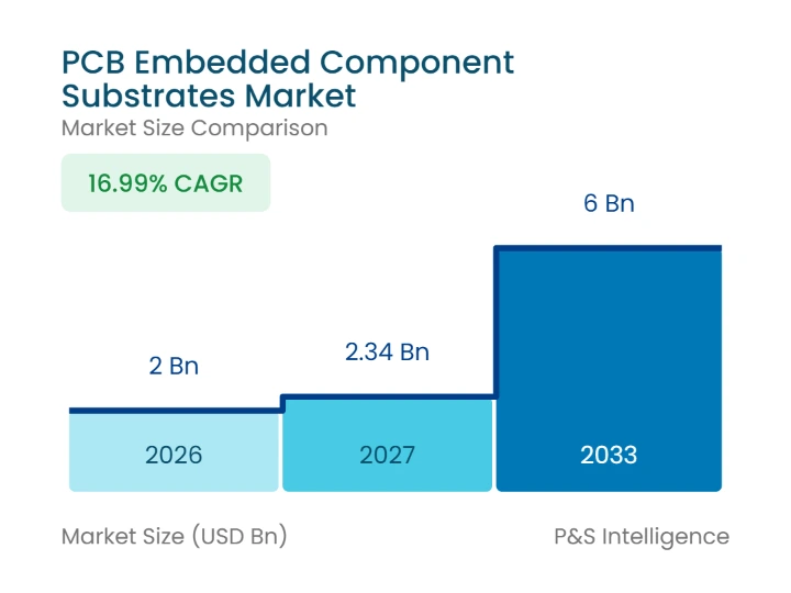
The global PCB embedded component substrates market size is estimated at USD 2.00 Billion in 2026 and is projected to reach USD 2.34 Billion in 2027. Revenue is expected to climb to USD 6.00 Billion by 2033, advancing at a CAGR of 16.99% during 2027-2033. AI server board designers and automakers fitting silicon carbide inverters into tighter housings are the main buyers, because burying capacitors, inductors, and power dies inside the laminate frees surface area and shortens the current path. For fabricators, the commercial payoff depends on keeping embedding yields high enough to justify the price premium these boards carry.
Hyperscale operators building AI capacity now write the power-delivery specifications that most often bring embedded components into server boards. Lawrence Berkeley National Laboratory's June 2026 update for the U.S. Department of Energy estimates that data centers could use 11.8% of U.S. electricity by 2030, within a 9.5% to 15.3% scenario range. The estimate covers whole-facility load, yet every conversion loss between the rack and the processor scales with it. Placing regulators and decoupling capacitors inside the substrate, directly beneath the processor, is one of the few ways to cut that loss without adding board area.
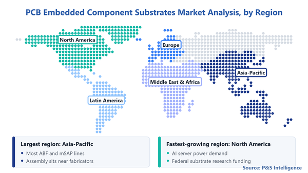
Asia-Pacific accounted for 62% of 2026 revenue, anchored by substrate lines in Taiwan, Japan, South Korea, and China that already run ABF build-up and fine-line processes. North America is projected to post the quickest regional growth, at a CAGR of 18.09% during 2027-2033, led by U.S. AI server programs. The contrast matters for suppliers in the PCB embedded component substrates market, since Asia-Pacific revenue grows by adding embedding to established high-volume lines, while North American revenue depends on winning new accelerator and power-electronics designs.
Key market insights
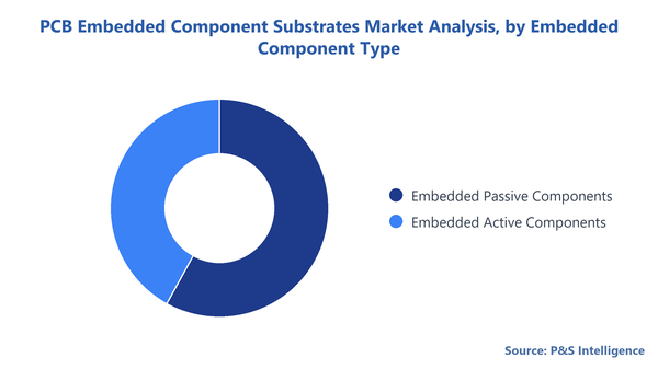
By embedded component type, embedded passive components held 58.0% in 2026, while embedded active components is projected to grow at an 18.59% CAGR during 2027-2033.
By substrate structure, embedded component packaging (ECP / organic) held 48.0% in 2026, while embedded trace & coreless substrates (ETS) is projected to grow at an 18.29% CAGR during 2027-2033.
By end-use application, automotive & EV mobility held 38.0% in 2026, while telecommunications & data infrastructure is projected to grow at an 18.79% CAGR during 2027-2033.
By geography, Asia-Pacific held 62.0% in 2026, while North America is projected to grow at an 18.09% CAGR during 2027-2033.
PCB Embedded Component Substrates Market Dynamics
Power-die embedding in build-up laminates is redefining how power modules are packaged
Power-module makers are starting to bury silicon carbide and gallium nitride dies inside organic build-up laminates in place of soldering them onto ceramic substrates and connecting them with bond wires. Removing the wire bonds shortens the current loop, which cuts switching losses and lets a module carry larger dies in a thinner package. That change can move part of the value in a power module from conventional packaging houses toward substrate fabricators with laser-via, plating, and lamination control, because the substrate itself becomes the package.
USI showcased the approach at PCIM Europe 2026 in May 2026, with a module that embeds SiC dies in multilayer ABF substrates and pairs them with ceramic insulation in a wire-bondless design housed in industry-standard power package formats. The company is aiming the design at electric mobility, AI data centers, and humanoid robotics. The standard outline matters commercially, since inverter and power-supply engineers can evaluate an embedded part without redesigning the surrounding board, which lowers the cost of a first trial order.
AI accelerator power delivery is driving passive embedding into package substrates
Each new AI accelerator generation draws more current at low core voltage, and the decoupling capacitors that steady that supply work best when they sit within millimeters of the die. Capacitors mounted on the board or on the package underside sit farther away and take up area that signal and power routing also needs. Package-substrate makers are responding by embedding capacitors in the core or build-up layers, which turns a commodity passive purchase into a higher-value substrate specification negotiated with the processor designer.
Elohim and Daeduck Electronics announced in January 2024 that they had embedded silicon capacitors of up to 1,000 nF/mm² inside Daeduck's FC-BGA substrate, with 2,000 nF/mm² in development, for data-center, mobile application-processor, and GPU and CPU packages. Capacitance at that density can let designers shrink board-level capacitor banks. For substrate fabricators, this kind of embedding ties the product to one processor platform, so a design win is likely to hold for much of that platform's production life.
Electric vehicle inverter redesigns are opening a power-substrate growth pathway
Automakers moving to 800-volt platforms and silicon carbide inverters need to shrink inverter volume and cut switching losses at the same time, and embedding the power dies inside a heavy-copper or build-up laminate addresses both goals. Loop inductance falls when dies, busbars, and capacitors share one laminated stack, which lets SiC devices switch faster with less voltage overshoot. Each inverter program that adopts embedding would create a multiyear substrate order tied to the vehicle platform's production run.
International Energy Agency data show that global electric car sales grew 20% to exceed 20 million in 2025, so one in four new cars sold was electric. That number sizes the vehicle platform base embedded power substrates could serve, not the adoption of embedding itself, as conventional power modules remain the incumbent inverter construction. The opportunity lies in converting a portion of that base. Substrate makers that pass automotive qualification for embedded SiC are better positioned to turn platform awards into recurring volume.
Material cost inflation and no-rework yields are constraining substrate margins
An embedded substrate carries its components inside the laminate, so a defect found after lamination scraps the board together with every capacitor, inductor, or die already buried in it. Fabricators therefore need known-good components and tightly controlled lamination, and they price that yield risk into each panel. Higher unit prices can slow conversion in cost-sensitive consumer designs, where a surface-mount layout still fits and the board-space saving does not justify the premium.
Schweizer Electronic warned in its first-quarter 2026 update, published on May 6, that a persistent rise in material prices and a tightening procurement situation were weighing on planning certainty. Embedded constructions buy the same copper and laminate as conventional boards plus the buried components, so a material price rise can land on a larger part of their cost base. Fabricators with long-term supply agreements and qualified alternative materials can protect margins more easily, while smaller shops may defer embedding projects until input prices settle.
Segmentation Outlook
Embedded Component Type
Embedded passive components accounted for 58% of PCB embedded component substrates market revenue in 2026, the larger of the two component types. MLCCs, thin-film resistors, and planar inductors were the first parts fabricators learned to bury, so their lamination recipes, component tolerances, and reliability data have the longest production history. A failed passive is also cheaper to scrap than a power die, which keeps yield losses tolerable at high volume. Smartphone module makers and server-board designers both specify passive embedding to free surface area, giving this category the widest base of design wins across consumer, computing, and automotive circuit boards.
Embedded active components are projected to expand the fastest, at a CAGR of 18.59% over 2027-2033, as SiC MOSFETs, GaN transistors, PMICs, and bare logic dies move inside the laminate. Power semiconductors gain the most from embedding because the current loop, and with it the switching loss, shrinks when the die sits within the board. Each buried die also carries more value than a buried capacitor, lifting substrate revenue per converted board. Inverter and server power-supply programs that qualify an embedded die tend to keep it for the platform's life, which favors fabricators with proven automotive and data-center qualification records.
Copyright P&S Intelligence. Reuse requires attribution under CC BY 4.0.
Substrate Structure
Embedded component packaging (ECP / Organic) substrates held 48% of 2026 revenue. These constructions use RCC, ABF build-up, or FR-4 cores with laser microvias, the same process steps most high-density interconnect lines already run, so a fabricator can add embedding without rebuilding its factory. That process continuity keeps conversion cost low for module makers in consumer, automotive, and industrial electronics, and it widens the pool of fabricators able to quote a design. Broad compatibility also lets OEMs embed passives and small actives in the same board, which makes ECP a common starting point for both system-in-package and compact power-module designs.
Embedded trace & coreless substrates (ETS) are expected to post the quickest growth in this axis, with a CAGR of 18.29% during 2027-2033. These substrates are built on a modified semi-additive process at line and space below 15 µm, the routing density that AI accelerator and high-performance computing packages require. Removing the core also thins the package and shortens vertical power paths, which helps when embedded capacitors must sit directly beneath a processor. Capacity added here favors fabricators that already run mSAP lines for ABF substrates, since the plating equipment, imaging tools, and process control carry over with limited retooling.
End-Use Application
Automotive & EV mobility accounted for 38% of 2026 revenue, the largest end-use share. Carmakers and their tier-one inverter, on-board charger, and DC-DC converter suppliers need power stages that survive vibration, humidity, and temperature cycling in confined spaces, and sealing dies or passives inside the laminate can protect them better than exposed solder joints. Automotive qualification can also take years, so a substrate approved for a platform typically ships for that vehicle's full production run. That long revenue tail keeps automotive orders at the top of fabricators' books even as server and consumer applications add volume over the forecast period.
Telecommunications & data infrastructure is set to grow fastest among end uses, at an 18.79% CAGR in 2027-2033. AI servers, network switches, and optical transceivers are raising current density and signal speed together, which moves power stages and capacitors directly under the processor. Samsung Electro-Mechanics signed a USD 1.12 Billion (KRW 1.5 Trillion) contract in May 2026 to supply silicon capacitors placed inside AI server GPU and HBM packages from 2027. Those are package components, yet the order shows processor makers paying to bring power-delivery parts closer to the die, the same need that embedded substrates serve inside the board.
The following segments are analysed in this report.
Embedded Component Type
Embedded Passive Components
MLCCs
Thin-film Resistors
Planar Inductors
Embedded Active Components
SiC MOSFETs
GaN Transistors
PMICs
Logic Bare Dies
Substrate Structure
Embedded Component Packaging (ECP / Organic)
Embedded Trace & Coreless Substrates (ETS)
Heavy Copper / Power Substrates
End-Use Application
Automotive & EV Mobility
Consumer Electronics & Wearables
Telecommunications & Data Infrastructure
Industrial, Medical & Aerospace/Defense
Geographical Outlook
Asia-Pacific PCB embedded component substrates market outlook
Asia-Pacific accounted for 62% of global revenue in 2026, a lead built on where substrates are fabricated and where the boards that use them are assembled. Taiwan, Japan, South Korea, and China host most of the world's ABF build-up and mSAP lines, and embedding is added as a process step on those same lines. Handset, wearable, and server-board assembly also sits nearby, so module makers can qualify an embedded substrate with a fabricator located close to their own production.
Figures from the Taiwan Printed Circuit Association and ITRI's Industry, Science and Technology International Strategy Center put Taiwan-headquartered makers at 35.6% of the global IC substrate market in 2025 and 41.3% of ABF substrates. These figures cover all IC substrates, including non-embedded types, yet they show where the process capability sits. Taiwan, home to the largest group of these substrate makers, is the region's largest national market, with Japanese fabricators strong in fine-pitch package substrates. Asia-Pacific should stay in front through 2033, though its share could narrow as AI and automotive programs elsewhere ask for capacity nearer final assembly.
North America PCB embedded component substrates market growth
North America is projected to grow fastest among regions, at a CAGR of 18.09% during 2027-2033, with the United States as the region's fastest-growing national market. Growth here depends on new system designs more than on existing volume. U.S. hyperscale operators are specifying power-dense AI server boards, and each accelerator generation opens new qualification slots in which embedded power stages and capacitors can displace surface-mount layouts. Automotive power-electronics programs add a second, slower-moving source of design wins.
The National Institute of Standards and Technology confirms that the CHIPS National Advanced Packaging Manufacturing Program finalized USD 300 million for advanced substrate and materials research at Absolics, Applied Materials, and Arizona State University. Those awards fund glass-core, silicon-core, and fan-out packaging work outside embedded component substrates, yet they widen the domestic base of substrate process know-how. If U.S. packaging capacity reaches volume, fabricators with North American lines would be better placed to win AI server and inverter programs that value shorter supply chains.
Copyright P&S Intelligence. Reuse requires attribution under CC BY 4.0.
Europe market analysis
Europe holds a smaller share than Asia-Pacific but is home to several early developers of power-die and component embedding, with production in Austria and Germany. Demand comes mainly from automotive tier-one suppliers and industrial drive makers that want compact, well-cooled power stages for inverters, on-board chargers, and motor controls. Engineering centers of German and French carmakers often specify the power module themselves, so a substrate designed into a European platform can follow that platform into production outside the region.
The European Automobile Manufacturers' Association recorded 1,880,370 battery-electric car registrations in the EU in 2025, a 17.4% share of new cars, up from 13.6% a year earlier. Those registrations measure the domestic vehicle base and say nothing direct about embedded substrates, yet they show why European power-electronics designers keep looking for denser, lower-loss inverter layouts. Fabricators holding automotive qualifications in the region stand to benefit as embedded SiC moves from demonstrators into series platforms, with timing set by carmakers' program decisions.
Latin America market analysis
Latin America contributes a modest share, and its demand comes from final assembly, with little local substrate fabrication. Mexico's automotive and electronics plants, many of them building for the U.S. market, buy finished modules and boards that can contain embedded substrates. The purchasing decision for those parts is usually made at the OEM's design center in the United States, Europe, or Asia, and the Mexican plant then receives the specified board through the OEM's supply chain.
Brazil's demand is tied to its domestic vehicle industry and industrial electronics. According to ANFAVEA, the Brazilian vehicle manufacturers' association, the country produced 2.644 million vehicles in 2025, including units built for export, 3.5% more than in 2024. That count sizes the assembly base, not embedded-substrate use. For substrate makers, the region matters mainly through the OEMs and electronics manufacturing services companies that specify parts centrally and assemble locally, so winning volume in Latin America usually means winning the design elsewhere first.
Middle East & Africa market analysis
The Middle East & Africa holds a modest position in the market and depends on imported boards and modules. The U.A.E. is the main point of interest, because its AI data-center campus projects will need server boards with dense power delivery once they are equipped. As per G42, the first 200-megawatt cluster of the 1-gigawatt Stargate UAE project in Abu Dhabi is expected to go live in 2026. Those servers are built elsewhere, so the region adds demand for embedded substrates indirectly, through orders placed with server OEMs in Asia and North America.
Local electronics manufacturing in the region remains limited, and few automotive or industrial plants there specify power modules themselves. Demand from the U.A.E. is therefore likely to follow data-center commissioning schedules, stepping up as each campus phase is fitted out with AI servers. Substrate suppliers reach these end users through global server and power-supply OEMs, which means regional demand shows up in their order books as part of broader AI server programs and not as distinct regional contracts.
The following geographies are analysed in this report.
The PCB embedded component substrates market is divided between two technology layers that compete in different ways. High-density package substrates with embedded capacitors or dies come from a limited group of Asian and European IC-substrate fabricators, because the ABF and mSAP lines involved require investments running into billions of dollars and each customer qualification can take many months. Power and heavy-copper embedding is more open, with specialist PCB makers competing on application engineering for inverter and charger designs. The structure is still evolving as AI and automotive programs push both layers toward larger, contract-backed capacity.
In package substrates, AT&S, Ibiden, Unimicron, Samsung Electro-Mechanics, and Shinko Electric Industries compete on line-and-space capability, embedding yield, and long-term capacity agreements with processor makers. Component makers such as TDK and Taiyo Yuden take a different route, building embedded modules around their own passives and power parts and selling them as finished devices. Schweizer Electronic, Würth Elektronik, and Meiko Electronics concentrate on board-level embedding for power-electronics and industrial designs, where close engineering support during qualification counts for more than scale.
For buyers, this structure means switching costs are high once a design is qualified. An AI board or inverter built around one fabricator's embedding process would normally need new reliability testing before moving to another source, which favors incumbents on running platforms. Share therefore changes hands mainly at new platform launches, when OEMs reopen qualification and fabricators with spare embedding capacity can compete for the next design. Embedded modules that component makers sell as finished parts follow component approval routes instead, so they can enter designs between platform launches.
Major Companies in PCB Embedded Component Substrates Market:
AT&S (Austria Technologie & Systemtechnik AG)
Taiyo Yuden Co. Ltd.
Schweizer Electronic AG
TTM Technologies Inc.
TDK Corporation
Ibiden Co. Ltd.
Unimicron Technology Corp.
Samsung Electro-Mechanics Co. Ltd.
Shinko Electric Industries Co. Ltd.
Kyocera Corporation
Würth Elektronik GmbH & Co. KG
Meiko Electronics Co. Ltd.
PCB Embedded Component Substrates Market News
In August 2026, Toyota Research Institute of North America, with Virginia Tech and MIRISE Technologies Corporation, won a 2026 R&D 100 Award for an embedded-die PCB traction inverter that uses six embedded 1-kV SiC MOSFET dies to deliver 173 kW at 97% efficiency. The award shows automotive research groups treating the embedded-die board as the inverter’s power stage.
In August 2026, AT&S Austria Technologie & Systemtechnik AG reported first-quarter 2026/27 revenue of USD 613.30 Million (EUR 549 million), up 40% currency-adjusted, and confirmed 45-55% full-year growth guidance. Its Kulim, Malaysia expansion builds on agreements with AMD and another technology customer, still subject to final conclusion, tying new substrate capacity to named processor demand.
In May 2026, TDK Corporation launched the FS3303, a 3 A micro point-of-load converter measuring 2.5 x 2.5 x 1.2 mm that houses the controller, driver, MOSFETs, and inductor in a 3D chip-embedded package, with a 3 A to 80 A family planned. Regulation placed beside AI edge and optical-module processors shortens the power path designers must route.
In January 2026, the Global Electronics Association released IPC-6921, setting qualification, performance, and acceptance requirements for wire-bonding and flip-chip organic IC substrates used in AI, high-performance computing, and automotive electronics, drawing on 246 technical experts. A shared acceptance standard can shorten substrate qualification between fabricators and OEMs.
Last Updated: October 2026
Frequently Asked Questions About This Report
How big is the PCB embedded component substrates market?+
The global PCB embedded component substrates market size is estimated at USD 2.00 Billion in 2026 and is projected to reach USD 2.34 Billion in 2027.
Why are components being embedded inside PCB substrates?+
AI server board designers and automakers fitting silicon carbide inverters into tighter housings are the main buyers, because burying capacitors, inductors, and power dies inside the laminate frees surface area and shortens the current path.
What are the challenges of embedded component PCBs?+
An embedded substrate carries its components inside the laminate, so a defect found after lamination scraps the board together with every capacitor, inductor, or die already buried in it.
Which type of embedded component is growing fastest?+
Embedded active components are projected to expand the fastest, at a CAGR of 18.59% over 2027-2033, as SiC MOSFETs, GaN transistors, PMICs, and bare logic dies move inside the laminate.
Which region leads the embedded component substrates market?+
Asia-Pacific accounted for 62% of global revenue in 2026, a lead built on where substrates are fabricated and where the boards that use them are assembled.
Which region is growing fastest in embedded component substrates?+
North America is projected to grow fastest among regions, at a CAGR of 18.09% during 2027-2033, with the United States as the region's fastest-growing national market.
Who makes embedded die and embedded component substrates?+
In package substrates, AT&S, Ibiden, Unimicron, Samsung Electro-Mechanics, and Shinko Electric Industries compete on line-and-space capability, embedding yield, and long-term capacity agreements with processor makers.
Want a report tailored exactly to your business need?
Leading companies across industries trust us to deliver data-driven insights and innovative solutions for their most critical decisions. From data-driven strategies to actionable insights, we empower the decision-makers who shape industries and define the future. From Fortune 500 companies to innovative startups, we are proud to partner with organisations that drive progress in their industries.
Client Testimonials
Working with P&S Intelligence and their team was an absolute pleasure – their awareness of timelines and commitment to value greatly contributed to our project's success. Eagerly anticipating future collaborations.
McKinsey & Company
India
Unmatched Standards
Our insights into the minutest levels of the markets, including the latest trends and competitive landscape, give you all the answers you need to take your business to new heights
Complete Data Security
We take a cautious approach to protecting your personal and confidential information. Trust is the strongest bond that connects us and our clients, and trust we build by complying with all international and domestic data protection and privacy laws