India Advanced Packaging Market Size & Opportunities Analysis - Growth Strategies, Competitiveness, and Forecasts (2026 - 2032)
This Report Provides In-Depth Analysis of the India Advanced Packaging Market Report Prepared by P&S Intelligence, Segmented by Packaging Type (Flip-Chip, Fan-Out Wafer-Level Packaging, Fan-In Wafer-Level Packaging (FI-WLP), 2.5D/3D IC Packaging, Embedded Die), Application (Consumer Electronics, Automotive, Telecommunications, Industrial Manufacturing, Healthcare & Medical Devices, Aerospace & Defense), and Geographical Outlook for the Period of 2019 to 2032
Explore the market potential with our data-driven report
India Advanced Packaging Market Outlook
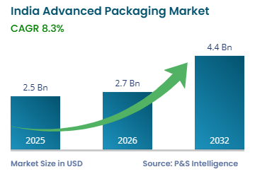
The Indian advanced packaging market values USD 2.5 billion in 2025, and it is projected to reach USD 4.4 billion by 2032, growing at a CAGR of 8.3% during 2026–2032. Advanced packaging technologies, including flip-chip, fan-out wafer-level packaging, and 2.5D/3D integration, are gaining significant traction in India as the country positions itself as a global semiconductor manufacturing hub. The market expansion is primarily driven by rising demand for miniaturized electronics, growing adoption of 5G technology, and substantial government investments under the India Semiconductor Mission.
As per government sources, India's semiconductor consumption is projected to more than double from USD 45–50 billion in 2024–2025 to USD 100–110 billion by 2030, creating substantial demand for advanced packaging solutions. The government has approved semiconductor projects worth over INR 1.55 lakh crore under the Semicon India Program, with facilities expected to produce 91 million chips daily once operational. According to the India Brand Equity Foundation, India became the world's third-largest packaging market in September 2024, surpassing Japan.
The rapid proliferation of 5G technology and internet of things devices is a primary driver for advanced packaging demand in India. In 2024, the penetration of smartphones in India reached 85.5% of households, with three out of every four smartphones shipped being capable of 5G technology. Further, as of June 2025, India has 1,002.85 million internet subscribers. This expanding digital ecosystem requires advanced semiconductor packaging solutions that deliver higher performance in smaller form factors. Fan-out wafer-level packaging and flip-chip technologies are particularly suited for 5G RF front-end modules and IoT sensors, driving their adoption across the Indian market.
India Advanced Packaging Market Dynamics
Growing Automotive Electronics Demand Is Main Market Trend
According to the Society of Indian Automobile Manufacturers, automobile production in India rose from 28,439,036 units in 2023–24 to 31,034,174 units in 2024–25.
Moreover, the Indian electric car market recorded a sale of 19,778 units in 2023, and it is projected to reach 430,603 units by the year 2030.
The integration of advanced driver assistance systems, battery management systems, and connected vehicle technologies is driving semiconductor content per vehicle significantly higher.
Stricter safety regulations, such as Bharat NCAP, are encouraging automakers to adopt ADAS features, including adaptive cruise control, automatic emergency braking, and blind-spot detection.
This continues to boost the demand for LiDAR sensors and radar chips and, in turn, for advanced semiconductor packaging.
Advanced packaging solutions like flip-chip, system-in-package, and embedded die technologies are essential for meeting the reliability, thermal management, and performance requirements of automotive applications.
Government Initiatives Are Boosting Industry Development
The Government of India has launched comprehensive initiatives to develop a domestic semiconductor ecosystem, directly benefiting the advanced packaging sector.
The Semicon India Programme has an outlay of INR 76,000 crore for developing semiconductor and display manufacturing capabilities.
The scheme extends fiscal support of 50% of the project cost for semiconductor fabs and 30% for ATMP/OSAT facilities.
As of June 2024, incremental investments of INR 8,390 crore have been made under the PLI scheme for large-scale electronics manufacturing, leading to production worth INR 5,14,960 crore.
The Design Linked Incentive scheme provides product design incentives of up to 50% of eligible expenditure and deployment-linked incentives of 4–6% on net sales for five years.
Six semiconductor manufacturing projects have been approved under the India Semiconductor Mission, including one fabrication facility and five ATMP/OSAT units, with cumulative investments of approximately INR 1,55,700 crore.
Data Center Expansion and AI Adoption Are Creating Market Opportunities
India's data center capacity has grown from 590 MW in 2019 to approximately 1.4 GW in 2025, with projections to reach 8 GW by 2030.
The India AI Mission has procured over 34,371 GPUs through two tender rounds, with approximately half already installed as of mid-2025.
Data center power demand in India is expected to grow nearly five times to 57 TWh by 2030, driven by AI workloads, cloud computing, and hyperscale deployments.
Reliance Industries has announced plans for a 3-GW AI data center campus in Jamnagar, Gujarat, with investments of USD 30 billion.
AWS, Microsoft, and Google have collectively pledged more than USD 15 billion for new data center capacity around Mumbai, Chennai, and Hyderabad.
This rapid data center expansion requires advanced packaging technologies, such as 2.5D/3D integration, high-bandwidth memory, and chiplet architectures, to meet the performance and power efficiency requirements of AI and high-performance computing workloads.
India Advanced Packaging Market Segmentation Analysis
Packaging Type Analysis
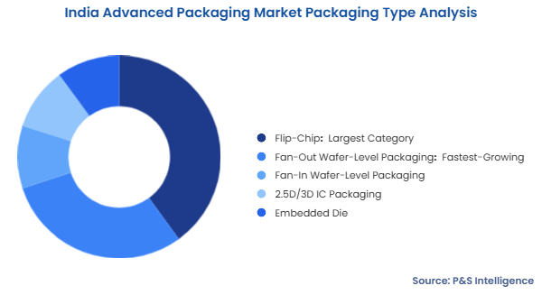
The flip-chip category holds the largest share in the Indian advanced packaging market in 2025, of 40%. Flip-chip technology enables direct electrical connection between the die and package carrier through solder bumps, offering superior thermal management, higher I/O density, and reduced signal loss. The technology is widely adopted in processors, graphics processing units, and networking chips used in smartphones, data centers, and high-performance computing applications. Major semiconductor companies operating in India, including those with design centers in Bengaluru and Hyderabad, rely extensively on flip-chip packaging for their advanced products.
Fan-out wafer-level packaging is expected to witness the highest CAGR, of 8.5%, during 2026–2032, driven by increasing demand for compact, high-performance devices. FO-WLP enables higher I/O density without increasing die size, making it ideal for mobile applications, RF front-end modules, and IoT devices. The technology offers a smaller package footprint, improved thermal and electrical performance, and cost advantages over traditional substrate-based packaging. With India's smartphone market reaching 153 million units in 2024 and 5G penetration accelerating, FO-WLP adoption is expected to grow significantly across the consumer electronics category.
The consumer electronics category dominates the Indian advanced packaging market in 2025, holding 35% share. The demand for consumer electronics, including smartphones, tablets, wearables, and smart home devices, continues to drive the need for advanced packaging solutions that enable smaller form factors and enhanced performance. The production of mobile phones surged to INR 4,22,000 crore in the fiscal year 2024–25, with exports exceeding INR 1,29,000 crore. Prominent global companies, including Apple, Samsung, and Xiaomi, have set up manufacturing operations in India, thereby increasing the demand for embedded solutions. As of November 2024, the investments committed under the PLI scheme reached INR 1.61 lakh crore, rising to around INR 1.76 lakh crore in 2025.
The automotive category is projected to grow at the highest CAGR during the forecast period, fueled by the rapid adoption of electric vehicles and advanced driver assistance systems. The increasing semiconductor content per vehicle, driven by electrification, connectivity, and autonomous driving features, is creating substantial demand for automotive-grade advanced packaging. The growing Indian EV battery market is driving demand for battery management ICs and power electronics that require advanced packaging technologies.
These applications are covered:
Consumer Electronics (Largest Category)
Automotive (Fastest-Growing Category)
Telecommunications
Industrial Manufacturing
Healthcare & Medical Devices
Aerospace & Defense
Others
Drive strategic growth with comprehensive market analysis
India Advanced Packaging Market Geographical Analysis
Gujarat Advanced Packaging Market Size
Gujarat holds the largest share in the Indian advanced packaging market in 2025, of 25%. The state has emerged as India's semiconductor manufacturing hub, hosting multiple high-profile projects in Dholera and Sanand industrial zones. Tata Electronics is developing India's first semiconductor fabrication facility in Dholera with an investment of USD 11 billion, expected to have a capacity of 50,000 wafers per month by 2027. The facility will produce chips for automotive, telecommunications, and artificial intelligence applications.
Sanand has become the focal point for ATMP and OSAT facilities, with Micron Technology establishing its first semiconductor assembly and test unit in India with investments proposed at USD 2.8 billion. The state's Dholera Special Investment Region and Sanand industrial clusters anchor this growth, hosting Kaynes Semicon's INR 3,307 crore facility, CG Power-Renesas' INR 7,600 crore joint venture, and complementing Micron's USD 2.75 billion assembly plant that represents India's first major international OSAT investment.
Tamil Nadu Advanced Packaging Market Forecast
Tamil Nadu is projected to witness the highest CAGR, of 8.4%, during 2026–2032, driven by its established electronics manufacturing ecosystem and strategic port connectivity. Chennai serves as a critical data center hub, with approximately 14.5% of India's total data center capacity. The state government unveiled the Tamil Nadu Automotive Future roadmap in June 2025 to position the state as a global EV innovation hub, including mobility innovation funds for R&D in battery chemistry and advanced EV technologies. Dedicated R&D zones in Chennai and Coimbatore are being developed to support semiconductor and advanced packaging innovation.
VinFast signed a MoU with the Tamil Nadu government in January 2024 to invest USD 2 billion for an EV project in Thoothukudi, with USD 500 million committed for the first phase targeting 150,000 units annually. Murata, a Japanese company, is building a factory at OneHub Chennai Industrial Park to produce multilayer ceramic capacitors, strengthening the state's semiconductor component ecosystem. The presence of major automotive manufacturers and electronics companies, combined with skilled workforce availability and port infrastructure, positions Tamil Nadu as a high-growth market for advanced packaging applications.
These states are covered:
Gujarat (Largest State Market)
Tamil Nadu (Fastest-Growing State Market)
Karnataka
Maharashtra
Assam
Uttar Pradesh
Rest of India
India Advanced Packaging Market Share
The Indian advanced packaging market is moderately consolidated, with the top five players collectively holding approximately 60% of the market share in 2025. The market is characterized by a mix of global semiconductor giants establishing local facilities and domestic companies building indigenous capabilities. International players dominate the high-end advanced packaging category, while domestic companies are rapidly building capacity in assembly, testing, and traditional packaging.
The competitive landscape is evolving rapidly as the India Semiconductor Mission catalyzes new entrants and strategic partnerships. Tata Electronics, through its collaboration with Taiwan's Powerchip Semiconductor Manufacturing Corporation, is positioning itself as a vertically integrated player across the semiconductor value chain. Kaynes Semicon achieved a significant milestone in July 2025 by delivering India's first commercially packaged prototype chip to U.S.-based Alpha & Omega Semiconductor, demonstrating indigenous OSAT capabilities meeting global standards.
Strategic partnerships between Indian and global companies are accelerating technology transfer and capability building. CG Power's joint venture with Renesas Electronics and Stars Microelectronics combines domestic manufacturing presence with established Japanese and Thai semiconductor expertise. In March 2025, Infineon Technologies signed an MoU with the Automotive Research Association of India to develop advanced semiconductor solutions for the automotive sector, focusing on EV inverters, vehicle control units, and ADAS technologies. The market is expected to witness further consolidation as companies seek to strengthen technological capabilities and secure anchor customers.
Key India Advanced Packaging Companies:
Tata Electronics Private Limited
Micron Technology Inc.
Kaynes Semicon Private Limited
CG Semi Private Limited
HCL Technologies Ltd.
MosChip Technologies Limited
SPEL Semiconductor Ltd.
Suchi Semicon Private Limited
ASM Technologies Limited
L&T Semiconductor Technologies Ltd.
Tessolve Services Pvt. Ltd.
Continental Device India Limited
Vedanta Limited
3D Glass Solutions Inc.
Polymatech Electronics
India Advanced Packaging Market News
In October 2025, Kaynes Semicon shipped India's first commercially packaged multi-chip module with complex 17-die intelligent power modules for automotive applications from its Sanand OSAT facility to U.S.-based Alpha & Omega Semiconductor.
In September 2025, UST and Kaynes Semicon announced a joint venture to build an INR 3,330 crore advanced packaging facility, expanding indigenous manufacturing capabilities.
In September 2024, the government approved Kaynes Semicon's INR 3,307 crore OSAT facility in Gujarat with a capacity of 6.3 million chips per day, becoming the fifth major semiconductor project under the India Semiconductor Mission.
In September 2024, Henkel Adhesive Technologies announced plans to support India's semiconductor ecosystem by providing adhesive solutions for semiconductor packaging, including die-attach pastes, encapsulation materials, and underfills.
In August 2024, Tata Electronics broke ground on its greenfield OSAT facility in Jagiroad, Assam, with an investment of INR 27,000 crore, expected to create over 27,000 direct and indirect jobs.
In March 2024, Prime Minister Narendra Modi laid foundation stones for three semiconductor projects worth INR 1.25 lakh crore, including Tata's facilities in Gujarat and Assam, signaling India's commitment to becoming a global semiconductor manufacturing hub.
In February 2024, the cabinet approved semiconductor projects by Tata Electronics in Dholera and Mori gaon, and CG Power's joint venture in Sanand, with combined investments exceeding INR 35,000 crore.
Want a report tailored exactly to your business need?
Leading companies across industries trust us to deliver data-driven insights and innovative solutions for their most critical decisions. From data-driven strategies to actionable insights, we empower the decision-makers who shape industries and define the future. From Fortune 500 companies to innovative startups, we are proud to partner with organisations that drive progress in their industries.
Client Testimonials
Working with P&S Intelligence and their team was an absolute pleasure – their awareness of timelines and commitment to value greatly contributed to our project's success. Eagerly anticipating future collaborations.
McKinsey & Company
India
Unmatched Standards
Our insights into the minutest levels of the markets, including the latest trends and competitive landscape, give you all the answers you need to take your business to new heights
Complete Data Security
We take a cautious approach to protecting your personal and confidential information. Trust is the strongest bond that connects us and our clients, and trust we build by complying with all international and domestic data protection and privacy laws