Semiconductor & IC Packaging Materials Market Size & Share Analysis - Trends, Drivers, Competitive Landscape, and Forecasts (2026 - 2032)
This Report Provides In-Depth Analysis of the Semiconductor & IC Packaging Materials Market Report Prepared by P&S Intelligence, Segmented by Material Type (Die Attach Adhesive, Encapsulant, Epoxy Molding Compound, Solder Ball, Underfill), Packaging Type (Ball Grid Array, Chip Scale Package, Flip Chip, Quad Flat No-Lead, Wafer-Level Packaging), Sales Channel (Direct Sales, Distributor Sales, Online Channels), Application (Automotive, Consumer Electronics, Healthcare, Industrial, Telecommunication), and Geographical Outlook for the Period of 2021 to 2032
Semiconductor & IC Packaging Materials Market Size Estimation
Key Highlights
Study Period
2021 - 2032
Market Size in 2025
USD 46.60 Billion
Market Size in 2026
USD 51.51 Billion
Market Size by 2032
USD 96.50 Billion
Projected CAGR
10.95%
Largest Region
Asia-Pacific
Fastest Growing Region
Asia-Pacific
Market Structure
Semi-Fragmented
Market Size
Explore the market potential with our data-driven report
Semiconductor & IC Packaging Materials Market Overview
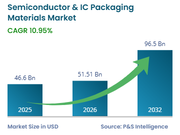
The global semiconductor and IC packaging materials market size was USD 46.60 billion in 2025 and is estimated at USD 51.51 billion in 2026. It is forecast to reach USD 96.50 billion by 2032, with a CAGR of 10.95%. Demand is shifting toward materials that can support denser connections, larger packages, higher power loads, and reliable assembly of multiple chips in one system.
The commercial opportunity extends across die attach adhesives, encapsulants, epoxy molding compounds, solder balls, and underfills, as well as the broader substrate and interconnect ecosystem. Package designers need these inputs to work together through bonding, molding, thermal cycling, and final operation. A material that performs well in isolation can still be unsuitable if it causes package warpage, weak adhesion, excessive signal loss, or poor manufacturing yield.
Artificial intelligence hardware, high bandwidth memory, automotive electronics, and power devices are increasing the value of qualified packaging materials. Larger and more complex packages create demand for tighter material tolerances and closer collaboration between suppliers and assembly partners.
The market spans design centers, materials suppliers, assembly plants, and device producers across the world. Asia-Pacific is the largest and fastest-growing region in the available comparable market studies.
Key Market Insights
By material type, the analysis groups die attach adhesives, encapsulants, epoxy molding compounds, solder balls, and underfills.
By packaging type, the analysis covers ball grid array, chip scale package, flip chip, quad flat no-lead, and wafer-level packaging.
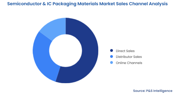
By sales channel, direct sales, distributor sales, and online channels serve different qualification and order-size needs.
By application, the analysis covers automotive, consumer electronics, healthcare, industrial, and telecommunication uses.
By geography, Asia-Pacific leads the five-region analysis in size and projected growth.
Semiconductor & IC Packaging Materials Market Trends and Growth Drivers
AI processors and advanced memory raise material performance requirements
semiconductor and IC packaging materials market growth is being driven by packages that combine powerful processors, high bandwidth memory, and dense interconnects. Greater package area and power density increase exposure to warpage, thermal stress, and interconnect failure. Suppliers therefore face rising demand for stable die attach, low stress molding and encapsulation, dependable underfill, and effective heat removal. A 2025 foundry annual report describes continued development of advanced packaging and 3D chip stacking, but does not quantify sales of any material category.
The market growth can extend beyond a single premium package. As assembly lines adapt to finer pitches and more complex stacks, material consistency and process compatibility become purchasing criteria. Qualified formulations can reduce rework and support production yield, but adoption depends on successful testing in the complete package flow.
Domestic packaging programs open supplier qualification opportunities
The semiconductor and IC packaging materials industry has an opportunity to participate in regional advanced packaging buildouts. In the U.S., the Department of Commerce finalized USD 1.4 billion in National Advanced Packaging Manufacturing Program awards in January 2025, including support for substrate and materials research and a pilot facility. These projects can create additional venues for material evaluation, process integration, and supplier qualification. The awards are program funding, not a measure of packaging material sales or evidence that all planned capacity is operating.
Suppliers able to offer traceable inputs, technical support, and regional supply options may be better placed to work with new packaging lines. The semiconductor and IC packaging materials industry still depends on customer design wins, qualification timing, plant ramp-up, and unit economics rather than the headline value of public funding.
Finer interconnects and thermal control shape product development
Semiconductor and IC packaging materials industry trends are moving toward finer wiring, lower warpage, and thermal performance designed for particular package architectures. Advanced packages combine redistribution layers, fine-pitch interconnects, substrates, and protective materials. The range of materials illustrates why formulation changes must be assessed alongside interconnect geometry and process steps instead of as stand-alone substitutions.
Materials are also being adapted for fan-out, flip chip, and stacked devices. The resulting product development spans mechanical stability, signal integrity, and manufacturability. These semiconductor and IC packaging materials industry trends vary by device design, substrate, and assembly temperature.
Long qualification cycles and diversification costs slow substitution
New materials must survive reliability tests and run consistently on customer production equipment before they can replace an established formulation. A change to an adhesive, mold compound, or underfill can alter stress, moisture behavior, and bond integrity elsewhere in the package. The resulting qualification burden raises switching costs even when a candidate material offers a better single property.
Supply diversification adds a second restraint. Buyers seeking additional sources must build and qualify them well before a disruption occurs. Geographic diversification may improve resilience, but it can also add duplicate qualification work and near-term cost.
Semiconductor & IC Packaging Materials Market Segmentation Analysis
Material Type
The Semiconductor and IC Packaging Materials Market analysis groups the material offering into die attach adhesive, encapsulant, epoxy molding compound, solder ball, and underfill. Each group addresses a different failure mode or assembly step. Die attach chemistries secure the chip and influence heat transfer, while molding compounds and encapsulants protect it from mechanical and environmental stress. Underfills reinforce connections, and solder balls form external electrical joints.
Selection depends on package layout and operating conditions. Solder alloy, flux chemistry, particle size, and dispensing method must fit the interconnect pitch and assembly process. These technical distinctions do not establish which material group has the largest market share. Public sources provide no category values for this five-part material analysis.
Packaging Type
Packaging type divides the study into ball grid array, chip scale package, flip chip, quad flat no-lead, and wafer-level packaging. The same material can face different stresses in each format. Flip chip and wafer-level approaches place particular emphasis on fine interconnects and dimensional control, while larger substrates can make warpage and thermal paths more consequential.
Packaging architectures are demand contexts for materials, not interchangeable material categories. Fine-pitch interconnects require precise substrate and assembly processes, but this technical requirement does not identify the fastest-growing packaging type.
Sales Channel
Direct sales, distributor sales, and online channels form the analysis's route-to-market split. Direct relationships matter when a formulation must be co-developed, tested in a specific line, and supplied under strict change control. Distribution can support regional availability and smaller accounts, while online channels can help with standard products, samples, and early evaluation.
Channel choice is therefore tied to qualification depth, order size, and service requirements. A research purchase through an online portal does not imply that a high-volume advanced package will be sourced the same way. Public sources do not disclose the three channels' relative revenues or forecast CAGRs.
Application
The application split covers automotive, consumer electronics, healthcare, industrial, and telecommunication systems. Automotive powertrains and driver assistance functions put weight on thermal cycling and long operating life. Consumer devices require compact packages and high manufacturing throughput. Industrial and medical uses can impose distinct reliability and traceability requirements.
Telecommunication equipment adds demand for fast signal transmission and stable operation in network hardware. These use cases influence material specifications, but the accessible summary for this market series does not rank application revenues. Segment opportunities should be judged against the relevant device and package design, not inferred from the size of the downstream electronics industry.
The following categories have been analyzed in this report:
Material Type
Die Attach Adhesive
Silver Epoxy
Sintered Paste
Encapsulant
Liquid Encapsulant
Solid Encapsulant
Epoxy Molding Compound
Filled
Unfilled
Solder Ball
Lead-Free
Leaded
Underfill
Capillary Underfill
Molded Underfill
Packaging Type
Ball Grid Array
CBGA
MBGA
PBGA
Chip Scale Package
PoP
WLCSP
Flip Chip
Flip Chip BGA
Flip Chip CSP
Quad Flat No-Lead
DFN
LGA
Wafer-Level Packaging
Fan-In WLP
Fan-Out WLP
Sales Channel
Direct Sales
Distributor Sales
Online Channels
Application
Automotive
ADAS
Infotainment Systems
Powertrain
Consumer Electronics
Laptops
Smartphones
Android Smartphones
iOS Smartphones
Tablets
Android Tablets
iOS Tablets
Wearables
Healthcare
Diagnostic Equipment
Imaging Equipment
Wearable Medical Devices
Industrial
Automation Equipment
Power Tools
Robotics
Telecommunication
Base Stations
Network Equipment
Routers
Drive strategic growth with comprehensive market analysis
Semiconductor & IC Packaging Materials Market Geographical Analysis
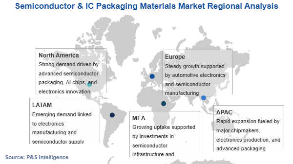
Asia-Pacific is assessed as both the largest and fastest-growing region for semiconductor and IC packaging materials. Comparable studies identify it in both positions, and its concentration of fabrication, assembly, testing, material production, and advanced packaging capability supports that assessment. Demand for AI accelerators, memory, consumer electronics, and power devices strengthens its outlook.
The Americas combine chip design and advanced computing demand with efforts to expand packaging capability. Local lines can give material suppliers additional places to validate complete process flows. Future material demand will depend on production ramps and supplier qualification rather than the announcement of new capacity alone.
Within Asia-Pacific, India is expanding assembly and test capacity. In July 2026, the government reported 12 approved semiconductor projects, including nine assembly, testing, marking, and packaging or outsourced assembly and test facilities across six states. Three of the approved projects had entered commercial production. The expanding project base can create qualification opportunities for material suppliers, but the government figures do not measure packaging-material purchases.
Within the Americas, the U.S. is developing domestic advanced packaging capacity. In September 2026, a packaging and test provider announced a second phase for its Arizona campus, with 60,000 square meters of additional cleanroom space planned in response to customer commitments. Construction of that phase is expected to begin in late 2027, so the announcement is a future-capacity indicator rather than current material revenue. The accessible summary for this market series does not provide a U.S. market share or growth rate.
The following geographies have been analyzed in this report.
North America
U.S.
Canada
Europe
U.K.
Germany
France
Italy
Spain
Rest of Europe
Asia-Pacific
China
India
Japan
Australia
South Korea
Rest of Asia-Pacific
Latin America
Mexico
Brazil
Rest of Latin America
Middle East & Africa
Saudi Arabia
U.A.E.
South Africa
Rest of Middle East & Africa
Semiconductor & IC Packaging Materials Market Share Analysis
The semiconductor and IC packaging materials industry is semi-fragmented, with formulation specialists, substrate manufacturers, interconnect suppliers, and firms that offer several material families. Competition is shaped by qualification history, process compatibility, reliability data, and the ability to supply at scale.
Supplier types span formulation specialists, substrate producers, and interconnect-material providers. They address different parts of the package bill of materials. A broad roster should not be interpreted as evidence that each participant competes in every material category.
Product breadth and close technical support can improve a supplier's position when packages require several materials to pass qualification together. At the same time, a specialist can retain a defensible position where its formulation or process expertise solves a narrow reliability problem. Supplier share can change as new package designs enter volume production, but the direction and magnitude cannot be estimated from product announcements alone.
Packaging and test companies occupy a related but distinct position. Some providers develop substrates while purchasing other materials, so their service revenue cannot be compared directly with a merchant adhesive or solder supplier's sales. The service-material distinction matters when reading broad company lists alongside the study's undisclosed market-share tables.
Top Companies in Semiconductor & IC Packaging Materials Market:
Henkel AG & Co. KGaA
Sumitomo Bakelite Co. Ltd.
DuPont de Nemours Inc.
Indium Corporation
3M Company
Shin-Etsu Chemical Co. Ltd.
Resonac Corporation
NAMICS Corporation
Ajinomoto Fine-Techno Co. Inc.
IBIDEN CO. LTD.
Kyocera Corporation
Semiconductor & IC Packaging Materials Market News
In August 2026, Henkel launched a conductive die attach film series for high-power semiconductor packages. The company reported thermal conductivity above 8 W/m-K and positioned the film for AI, communications, and other demanding applications.
In May 2026, Sumitomo Bakelite Co. Ltd. announced that trial launches of its liquid encapsulant series had begun in April. The company designed the material for low warpage and package reliability as chiplet and stacked designs increase package size.
In April 2026, Kyocera Corporation announced commercialization of a multilayer ceramic core substrate for advanced AI semiconductor packages. The company said the design targets package warpage and finer wiring.
Frequently Asked Questions About This Report
Which materials are included in the market?+
The commercial opportunity extends across die attach adhesives, encapsulants, epoxy molding compounds, solder balls, and underfills, as well as the broader substrate and interconnect ecosystem.
Why can a packaging material fail qualification?+
A material that performs well in isolation can still be unsuitable if it causes package warpage, weak adhesion, excessive signal loss, or poor manufacturing yield.
What limits adoption of new packaging formulations?+
Qualified formulations can reduce rework and support production yield, but adoption depends on successful testing in the complete package flow.
How do semiconductor materials sales channels differ?+
Distribution can support regional availability and smaller accounts, while online channels can help with standard products, samples, and early evaluation.
Want a report tailored exactly to your business need?
Leading companies across industries trust us to deliver data-driven insights and innovative solutions for their most critical decisions. From data-driven strategies to actionable insights, we empower the decision-makers who shape industries and define the future. From Fortune 500 companies to innovative startups, we are proud to partner with organisations that drive progress in their industries.
Client Testimonials
Working with P&S Intelligence and their team was an absolute pleasure – their awareness of timelines and commitment to value greatly contributed to our project's success. Eagerly anticipating future collaborations.
McKinsey & Company
India
Unmatched Standards
Our insights into the minutest levels of the markets, including the latest trends and competitive landscape, give you all the answers you need to take your business to new heights
Complete Data Security
We take a cautious approach to protecting your personal and confidential information. Trust is the strongest bond that connects us and our clients, and trust we build by complying with all international and domestic data protection and privacy laws