Key Highlights
| Study Period | 2021 - 2032 |
| Market Size in 2025 | USD 2.14 Billion |
| Market Size in 2026 | USD 2.34 Billion |
| Market Size by 2032 | USD 3.74 Billion |
| Projected CAGR | 8.13% |
| Asia-Pacific | 77.00% |
| North America | 9.8% CAGR |
| Market Structure | gray-zone |

| Study Period | 2021 - 2032 |
| Market Size in 2025 | USD 2.14 Billion |
| Market Size in 2026 | USD 2.34 Billion |
| Market Size by 2032 | USD 3.74 Billion |
| Projected CAGR | 8.13% |
| Asia-Pacific | 77.00% |
| North America | 9.8% CAGR |
| Market Structure | gray-zone |
Explore the market potential with our data-driven report
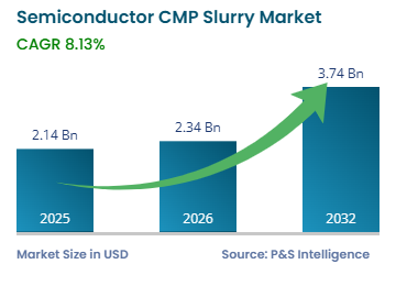
The Semiconductor CMP Slurry Market size was USD 2.14 billion in 2025 and is projected to reach USD 2.34 billion in 2026 and USD 3.74 billion by 2032, advancing at an 8.13% CAGR during 2026–2032. Demand grows with wafer starts and with the number of planarization steps required across transistor, interconnect, memory, and packaging flows.
Commercial competition occurs at the process level. A formulation must balance removal rate, selectivity, corrosion control, particle stability, and defect limits for a customer's film stack. For a stable process, requalification risk can outweigh a lower unit cost. Global wafer-fabrication-materials revenue reached USD 45.8 billion in 2025, up 5.4%, within a USD 73.2 billion semiconductor-materials total, according to SEMI. Those figures cover all wafer-fabrication materials, but they show the scale of the recurring consumables base in which slurry suppliers compete.
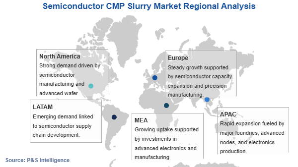
Asia-Pacific held 77% of the Semiconductor CMP Slurry Market share in 2025, supported by its concentration of foundry, logic, and memory capacity. North America is the fastest-growing region at a 9.8% CAGR through 2032 as new fabs and supply-chain investments advance toward qualification. The commercial result depends on utilization and ramp timing. Announced capacity does not create slurry revenue until a process is installed, qualified, and producing wafers.
Semiconductor CMP Slurry Market growth is driven by the addition of wafer capacity and the repeated use of planarization across multilayer device structures. SEMI's World Fab Forecast placed global semiconductor capacity at 33.6 million 200 mm-equivalent wafers per month in 2025, up 6.6%, while identifying 18 fabs expected to begin construction during the year. Construction starts do not equal operating output. They enlarge the pipeline of lines that will need process chemicals when equipment installation and qualification are complete.
The mechanism extends beyond a simple wafer-volume increase. Each new film stack creates requirements for removal rate, selectivity, corrosion behavior, and defect control. A slurry that performs on one metal or dielectric combination cannot be assumed to transfer unchanged to another. Suppliers gain recurring volume only after they support trials, stabilize the process window, and pass the customer's qualification. Ramp timing is the practical boundary on demand.
The opportunity for the semiconductor CMP slurry industry is moving into packaging processes that require controlled preparation of bonding and interconnect surfaces. Global semiconductor assembly and packaging equipment sales grew to $6.0 billion in 2025 and are projected to reach $6.7 billion in 2026. Equipment spending is a capacity proxy, not a slurry-revenue measure, yet it indicates that more packaging lines are being equipped for complex integration work.
Hybrid bonding, through-silicon vias, redistribution layers, and polymer surfaces create separate material combinations and defect thresholds. FUJIFILM Corporation launched a slurry for copper and oxide surfaces used in hybrid bonding in September 2025, with adoption disclosed at one unnamed device manufacturer. The single disclosed adoption confirms commercial availability without proving broad use. Buyers can evaluate packaging-specific formulations alongside pads and cleaners, while suppliers must earn each process position separately.
Semiconductor CMP slurry industry trends increasingly center on material-specific chemistry. Copper remains embedded in multilayer interconnect and packaging structures, but cobalt, ruthenium, polymers, and mixed copper-oxide surfaces impose different corrosion and selectivity conditions. TSMC reported that fine-pitch copper bump technology for 2 nm silicon entered volume production in 2025. The node reference establishes current copper use in packaging and does not specify slurry volume.
Product design is moving toward narrower platforms aligned with a surface and integration flow. A mixed surface can require the slurry to remove one film at a controlled rate while protecting the adjacent material and limiting residues. Suppliers able to tune abrasives and chemical additives together can address that requirement, then support evaluation near the customer's line. Portfolio breadth helps only when individual formulations meet the required process window.
Qualification friction restrains substitution even when several suppliers can formulate for the same broad material class. Particle distribution, surface chemistry, additive stability, and filtration interact with the pad and tool. A change intended to improve removal can also alter scratches, dishing, erosion, or residue. Buyers must test these effects on the relevant structure before replacing a validated slurry, which lengthens the route from sample approval to production volume.
Intellectual-property boundaries add another constraint. Taiwan's Intellectual Property and Commercial Court upheld one Entegris, Inc. acidic colloidal-silica patent on July 14, 2026, and China's National Intellectual Property Administration upheld a related patent on August 10, 2026. The decisions concern validity rather than product performance. Protected claims can raise design-around costs for nearby formulations, while dual sourcing remains possible where suppliers qualify distinct chemistry.
Colloidal silica held 52.0% of revenue in 2025. Its position draws on qualification across recurring dielectric and finishing steps. Qnity Electronics Inc.'s current portfolio documents colloidal-silica use across four named process families, covering interlayer dielectrics, shallow trench isolation, polysilicon, and post-metal buff. The four-family portfolio establishes process breadth without assigning Qnity the category share and shows why silica chemistry can serve multiple production steps.
Ceria is projected to advance at a 9.4% CAGR during 2026–2032. Its growth driver is the control of particle design and oxide selectivity for shallow trench isolation and dielectric polishing. AGC Inc. integrates abrasive-particle design with finished-slurry formulation, which supports tuning for specific silicon-based films. The capability statement belongs to AGC and does not establish market-wide yield performance.
Copper and copper barrier accounted for 45.0% in 2025. Repeated metallization layers sustain bulk-copper and barrier-planarization demand across a device flow. IBM Research demonstrated a 14 nm logic technology with 15 levels of copper metallization. The 15-level count applies only to the disclosed IBM design and illustrates how a multilayer stack can create recurrent copper-processing requirements.
New metals and advanced-packaging surfaces are forecast to expand at an 11.6% CAGR during 2026–2032. The driver is the arrival of distinct interfaces involving cobalt, ruthenium, hybrid bonding, through-silicon vias, polymers, and glass. Commercial platforms now separate formulations by these surfaces, allowing customers to qualify selectivity and defect performance for each packaging flow.
Logic generated 44.0% of revenue in 2025. Its position is supported by advanced-node capacity and the interconnect complexity of high-performance devices. SEMI's World Fab Forecast projected capacity at 7 nm and below to increase 16% to 2.2 million 200 mm-equivalent wafers per month in 2025. Capacity differs from utilization and expands the production base requiring tightly controlled planarization after qualification.
Advanced packaging is projected to grow at an 11.2% CAGR during 2026–2032. The driver comes from new hybrid-bonding, TSV, and redistribution-layer process capacity. Global packaging and assembly equipment sales rose 19.6% to USD 6.0 billion in 2025, SEMI equipment statistics show. The equipment figure measures investment activity. A larger installed equipment pool creates more packaging lines where CMP formulations can be evaluated.
The 300 mm category held 78.0% in 2025. Its scale concentrates high-volume logic and memory production on a common wafer format. SEMI's second-quarter 2026 outlook tracked 413 300 mm fabs and production lines worldwide, including research and pilot lines. The count covers facilities at different lifecycle stages, but it demonstrates the breadth of the installed and planned platform served by compatible CMP consumables.
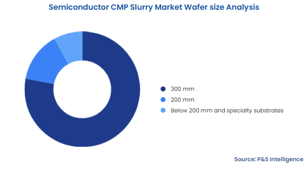
The same 300 mm category is projected to grow at an 8.7% CAGR during 2026–2032. Its forward driver is continued capacity installation. SEMI's second-quarter outlook expected total installed 300 mm capacity to increase 7% in 2026. New capacity adds slurry demand only after equipment move-in, process qualification, and wafer ramps.
Foundries held 47.0% in 2025. Their position derives from a multi-customer production base spanning advanced and mature logic processes. SEMI's World Fab Forecast projected foundry capacity to rise 10.9% to 12.6 million 200 mm-equivalent wafers per month in 2025. The capacity measure differs from utilization and indicates the scale of process lines that can consume qualified slurry repeatedly.
Outsourced semiconductor assembly and test providers are forecast to grow at a 10.9% CAGR during 2026–2032. Their driver is the expansion of packaging flows that add planarization to hybrid-bonding, TSV, interposer, and redistribution-layer work. New packaging equipment makes these providers a separate qualification and support point for slurry suppliers.
Drive strategic growth with comprehensive market analysis
Asia-Pacific generated 77% of global Semiconductor CMP Slurry Market revenue in 2025 and is projected to expand at an 8.2% CAGR during 2026–2032. The region's position is cumulative. Taiwan, South Korea, Japan, China, and Southeast Asian manufacturing centers combine foundry, memory, logic, wafer, and materials operations that have built qualification histories over multiple process generations. Long qualification histories support recurring purchases because each active layer and film stack uses a validated combination of slurry, pad, cleaning, filtration, and tool settings.
Regional scale is reinforced by continued 300 mm investment. SEMI's second-quarter outlook expected global installed 300 mm capacity to rise 7% in 2026 and tracked 413 fabs and production lines. The global figures cannot prove Asia-Pacific revenue. The same dataset identifies China, Taiwan, South Korea, and Japan as major capacity centers. Asia-Pacific's lead could narrow if utilization weakens across its largest fabs or if new advanced-node and packaging capacity reaches production faster in other regions.
North America is the fastest regional contributor to Semiconductor CMP Slurry Market growth, with a 9.8% CAGR projected for 2026–2032 from a 12.1% share in 2025. Its mechanism is capacity arriving rather than a larger inherited manufacturing base. U.S. commitments covered 17 new fabs and eight supply-chain and advanced-packaging facilities across 22 states, according to a January 2025 Department of Commerce report. These commitments sit at different stages and do not establish operating output for North America.
The project pipeline matters to slurry suppliers because a new line creates qualification work before it creates recurring orders. Supplier planning must follow project milestones because demand materializes only after equipment installation, process qualification, and ramp. The United States anchors the disclosed construction pipeline, but it does not receive a separate country treatment here. North America's forecast position would weaken if projects are delayed, capacity ramps below plan, or materials qualification remains tied to imports without local support.
China held 35.0% of Asia-Pacific revenue in 2025, making it the largest approved country market. Installed scale is the principal reason. SEMI's World Fab Forecast projected semiconductor capacity at 10.1 million 200 mm-equivalent wafers per month in 2025 after 14% annual growth, nearly one-third of the global total. Capacity differs from production and slurry revenue, and the country's mix includes mature-node lines with different slurry intensity from advanced logic and memory facilities.
China's installed base creates a wide field for copper, barrier, dielectric, tungsten, and substrate qualifications. Domestic fabs can evaluate local and international formulations against the same process constraints, including selectivity, defects, residue, stability, and lot consistency. China's largest-country position could shift if utilization falls, new lines ramp slowly, or Taiwan and South Korea add higher-intensity logic and memory capacity faster.
China is also the fastest-growing approved country, with a 10.8% CAGR projected for 2026–2032. The growth mechanism differs from its scale advantage. Anji Microelectronics Technology (Shanghai) Co., Ltd. reports mass production of copper and barrier slurries and development of formulations for TSV and hybrid-bonding applications. The disclosure establishes one domestic supplier's process breadth and does not prove national self-sufficiency or a market-wide qualification rate.
Local formulation, sampling, and troubleshooting can shorten the physical distance between development teams and fabs, but customers still control qualification. Growth depends on domestic suppliers moving from trials into stable volume while international suppliers maintain service and production options. Export controls can redirect node investment and material choices without determining slurry revenue by themselves. China's fastest-country position would be vulnerable if localization stalls, fab utilization remains low, or packaging and advanced-memory investment accelerates more quickly elsewhere in Asia-Pacific.
Asia-Pacific
North America
Europe
Latin America
Middle East and Africa
Rest of Middle East and Africa
The semiconductor CMP slurry industry has a gray-zone competitive structure. Large global materials companies hold broad portfolios, established manufacturing networks, and long qualification histories, yet regional specialists can pursue process-specific qualifications. Competition occurs at the formulation and customer-process level. A buyer may use different suppliers for copper bulk, barrier, tungsten, dielectric, substrate, and packaging steps, distributing purchasing across several suppliers. Incumbency is powerful inside a qualified step, while purchasing power remains distributed across several steps and sites.
Entegris, Inc. competes through the combination of slurry chemistry, pads, filtration, contamination control, and process monitoring, with protected colloidal-silica chemistry reinforcing its formulation boundary. FUJIFILM Corporation extends copper-interconnect experience into mixed copper-oxide surfaces for hybrid bonding. Fujimi Incorporated emphasizes abrasive engineering and process-specific formulation across silicon and device layers. AGC Inc. links abrasive-particle design with finished slurry and post-CMP cleaning, giving it control over both particle and chemical choices. Integration depth, formulation precision, and the ability to diagnose defects across adjacent consumables distinguish these approaches.
Merck KGaA addresses planarization across front-end, interconnect, and packaging processes through a wider semiconductor-materials portfolio. Resonac Corporation differentiates through nano-ceria and its connection to other front-end and packaging materials. Anji Microelectronics Technology (Shanghai) Co., Ltd. competes through local qualification across copper, barrier, dielectric, tungsten, and emerging packaging uses. Soulbrain Co., Ltd. brings memory-process and nano-ceria coverage to Korean and regional customers. Regional proximity can speed sampling and troubleshooting, although every supplier still faces the customer's defect, consistency, and change-control requirements.
KCTech Co., Ltd. can coordinate slurry development with CMP equipment knowledge, which supports process troubleshooting at the tool-material interface. DONGJIN SEMICHEM CO., LTD. participates through localized oxide and metal slurry supply within Korea's semiconductor-materials base. Buyers also consider lot consistency, contingency supply, response time, and compatibility with pads, cleaners, and filters. Qualification strength remains local to a process, so success in one slurry category does not transfer automatically to another. The practical tradeoff is between global supply breadth and close process support. For entrants, the main barrier is earning stable production qualification without an installed performance history.
Want a report tailored exactly to your business need?
Request CustomizationLeading companies across industries trust us to deliver data-driven insights and innovative solutions for their most critical decisions. From data-driven strategies to actionable insights, we empower the decision-makers who shape industries and define the future. From Fortune 500 companies to innovative startups, we are proud to partner with organisations that drive progress in their industries.

Working with P&S Intelligence and their team was an absolute pleasure – their awareness of timelines and commitment to value greatly contributed to our project's success. Eagerly anticipating future collaborations.
McKinsey & Company
India
Our insights into the minutest levels of the markets, including the latest trends and competitive landscape, give you all the answers you need to take your business to new heights

We take a cautious approach to protecting your personal and confidential information. Trust is the strongest bond that connects us and our clients, and trust we build by complying with all international and domestic data protection and privacy laws


Customize the Report to Align with Your Business Objectives

Request the Free Sample Pages