Semiconductor Chemical Vapor Deposition Equipment Market Size & Share Analysis - Trends, Drivers, Competitive Landscape, and Forecasts (2026 - 2032)
This Report Provides In-Depth Analysis of the Semiconductor Chemical Vapor Deposition Equipment Market Report Prepared by P&S Intelligence, Segmented by Product Type (Atmospheric-Pressure Chemical Vapor Deposition, Low-Pressure Chemical Vapor Deposition, Plasma-Enhanced Chemical Vapor Deposition, High-Density Plasma Chemical Vapor Deposition, Metal-Organic Chemical Vapor Deposition), End User (Foundries, Integrated Device Manufacturers, Memory Device Manufacturers), and Geographical Outlook for the Period of 2021 to 2032
Semiconductor Chemical Vapor Deposition Equipment Market Size Estimation
Key Highlights
Study Period
2021 - 2032
Market Size in 2025
USD 17.6 Billion
Market Size in 2026
USD 18.5 Billion
Market Size by 2032
USD 26.2 Billion
Projected CAGR
5.9%
Largest Region
Asia-Pacific
Fastest-Growing Region
Asia-Pacific
Market Structure
Consolidated
Market Size
Explore the market potential with our data-driven report
Semiconductor Chemical Vapor Deposition Equipment Market Future Outlook
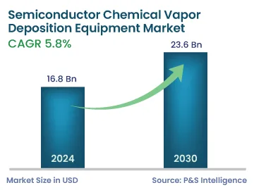
The semiconductor chemical vapor deposition equipment market size was USD 17.6 billion for 2025, and it will grow by 5.9% during 2026–2032, to reach USD 26.2 billion by 2032.
The upsurge in demand for microelectronic and semiconductor devices, technological advancements in the semiconductor industry, and the rise in the usage of semiconductor materials in AI programs such as IoT, autonomous vehicles, and AI-driven electronics are some of the prime factors contributing to the market growth. According to SEMI, global semiconductor equipment sales reached approximately USD 135 billion in 2025, reflecting strong growth in fab investments.
As semiconductor devices continue to scale down in size, the need for highly precise and controlled thin-film deposition processes is increasing, driving demand for advanced CVD equipment. In addition, the growing adoption of advanced packaging technologies, including heterogeneous integration and chiplet architectures, is further contributing to the demand for high-performance deposition systems.
Key Market Insights
The plasma-enhanced chemical vapor deposition category holds the largest market share, of 40%, in 2025, driven by its ability to deposit high-quality thin films at relatively low temperatures with uniformity.
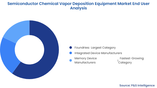
The foundries category holds the largest market share, of 60%, in 2025, driven by high-volume semiconductor manufacturing across industries.
The memory device manufacturers category will have the highest CAGR, of approximately 6.5%, driven by rising demand for high-density memory in data-intensive applications.
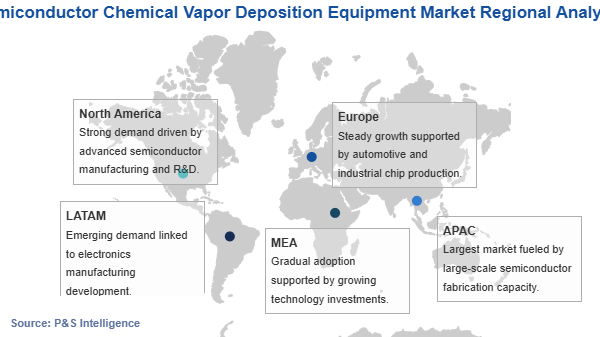
Asia-Pacific holds the largest market share, of 40%, in 2025, and it will have the highest CAGR, of approximately 6.8%, driven by its strong semiconductor manufacturing base.
China is the largest country in the Asia-Pacific semiconductor CVD equipment market, driven by strong government support, expanding wafer fabrication, and a focus on semiconductor self-sufficiency.
Semiconductor Chemical Vapor Deposition Equipment Market Trends & Drivers
Increasing Transition toward Advanced Nodes and 3D Device Architectures Are Key Trends
A defining trend in the semiconductor CVD equipment market is the rapid shift toward three-dimensional device architectures, including FinFET, gate-all-around (GAA) transistors, and 3D NAND memory structures. These advanced architectures require highly uniform and conformal thin-film deposition across complex, high-aspect-ratio geometries, increasing reliance on advanced CVD technologies such as PECVD and HDP-CVD. As device structures become more vertically integrated, precise material layering and defect control are becoming critical to maintaining performance and yield, reinforcing the importance of advanced deposition capabilities.
In addition, government-supported research and development initiatives are accelerating innovation in next-generation semiconductor technologies. Organizations such as the National Science Foundation and Semiconductor Research Corporation are actively funding advanced semiconductor research programs, while global institutions emphasize the growing role of semiconductors in energy-efficient applications, including electric vehicles and renewable energy systems. For instance, the U.S. government has allocated over USD 52 billion under the CHIPS and Science Act to strengthen domestic semiconductor manufacturing and innovation. These developments are driving the need for more sophisticated deposition technologies capable of supporting evolving device architectures and performance requirements.
Rapid Expansion of Semiconductor Manufacturing Capacity Is Biggest Driver
The expansion of global semiconductor manufacturing capacity is the primary driver of the CVD equipment market. Governments are increasingly prioritizing domestic chip production to reduce supply chain vulnerabilities and strengthen technological sovereignty, leading to substantial investments in new fabrication facilities across the United States, Europe, China, and India. For instance, the European Union has committed approximately EUR 43 billion under the European Chips Act to strengthen regional semiconductor manufacturing and reduce dependency on external supply chains.
According to the Semiconductor Industry Association, global semiconductor sales have exceeded USD 600 billion, reflecting the strong growth trajectory of the industry, while wafer fabrication capacity is projected to expand significantly through 2030. This sustained rise in production intensity is directly translating into increased demand for high-performance CVD equipment.
High Equipment Costs and Manufacturing Complexity Are Key Restraints
The semiconductor CVD equipment market faces constraints due to the high capital costs associated with advanced deposition systems and the increasing complexity of semiconductor manufacturing processes. CVD equipment requires precision engineering, advanced materials, and strict process control, making it one of the most expensive categories of semiconductor manufacturing equipment. These cost factors limit adoption primarily to large-scale fabrication facilities with substantial capital investment capabilities, restricting participation from smaller players and emerging markets.
In addition, the complexity of semiconductor manufacturing continues to increase as device architectures evolve. Maintaining uniform deposition across nanoscale and high-aspect-ratio structures requires advanced process control, specialized expertise, and continuous technological innovation. This not only increases operational challenges but also extends development cycles and raises the overall cost of ownership, creating significant barriers to entry and slowing broader equipment adoption across the semiconductor ecosystem.
Accelerating Demand for Compound Semiconductors and Power Electronics Is Biggest Opportunity
A significant opportunity in the semiconductor CVD equipment market lies in the rapid growth of compound semiconductors and power electronics, driven by the global transition toward electrification and energy efficiency. Technologies such as MOCVD are essential for depositing compound semiconductor materials, including gallium nitride (GaN) and silicon carbide (SiC), which are critical for high-performance electronic applications.
The International Energy Agency reports that global electric vehicle sales exceeded 17 million units in 2024, highlighting the accelerating demand for power semiconductors. In the U.S., the Department of Energy is actively supporting wide-bandgap semiconductor adoption through initiatives focused on power electronics innovation, aimed at improving energy efficiency in electric mobility and grid infrastructure. Governments in China, Japan, and South Korea are investing heavily in compound semiconductor manufacturing to support next-generation technologies, including 5G, renewable energy, and electric mobility. These factors are driving strong demand for advanced CVD equipment, particularly MOCVD systems, creating a major growth opportunity.
Semiconductor Chemical Vapor Deposition Equipment Market Segmentation Analysis
Product Type Analysis
The plasma-enhanced chemical vapor deposition category holds the largest market share in 2025, driven by its ability to deposit high-quality thin films at relatively low temperatures with uniformity. PECVD is widely used in dielectric layer deposition, passivation, and advanced node manufacturing processes. The increasing complexity of semiconductor devices and the need for precise thin-film control are reinforcing the dominance of PECVD systems.
The metal-organic chemical vapor deposition category will have the highest CAGR, of approximately 6.3%, driven by growing demand for compound semiconductors used in LEDs, power electronics, and high-frequency communication devices. Governments are actively supporting energy-efficient technologies, including LED lighting. The U.S. Department of Energy states that LED lighting can use at least 75% less energy than incandescent lighting, driving demand for MOCVD systems used in LED manufacturing.
The product types analyzed in this report are:
Atmospheric-Pressure Chemical Vapor Deposition (APCVD)
Low-Pressure Chemical Vapor Deposition (LPCVD)
Plasma-Enhanced Chemical Vapor Deposition (PECVD) (Largest Category)
High-Density Plasma Chemical Vapor Deposition (HDP-CVD)
Metal-Organic Chemical Vapor Deposition (MOCVD) (Fastest-Growing Category)
End User Analysis
The foundries category holds the largest market share, of 60%, in 2025, driven by their central role in high-volume semiconductor manufacturing for multiple industries, including consumer electronics, automotive, and telecommunications. Foundries continuously invest in advanced fabrication technologies and rely heavily on CVD systems for thin-film deposition across multiple process stages. According to industry data, more than 150 new semiconductor fabrication facilities are expected to come online globally between 2021 and 2030, with a significant share dedicated to foundry operations, supporting increased demand for advanced deposition equipment.
The memory device manufacturers category will have the highest CAGR, of approximately 6.5%, driven by increasing demand for high-density memory solutions in data-intensive applications such as AI, cloud computing, and high-performance computing. Memory fabrication, particularly DRAM and 3D NAND, requires a high number of deposition steps, increasing dependence on CVD technologies. The Government of South Korea has announced semiconductor investment plans exceeding USD 450 billion through 2047, with a strong focus on memory chip production, significantly boosting demand for advanced fabrication equipment including CVD systems.
Drive strategic growth with comprehensive market analysis
Semiconductor Chemical Vapor Deposition Equipment Market Geographical Analysis
Asia-Pacific Semiconductor Chemical Vapor Deposition Equipment Market Size
Asia-Pacific holds the largest market share, of 40%, in 2025, and it will have the highest CAGR, of approximately 6.8%, supported by the region’s high concentration of semiconductor fabrication capacity, particularly in advanced logic, memory, and foundry operations. Countries such as Taiwan, South Korea, China, and Japan play a central role in global semiconductor production, supported by well-established manufacturing ecosystems and continuous capacity expansion.
According to SEMI, China, Taiwan, and South Korea together accounted for approximately 79% of global semiconductor equipment spending in 2025. The presence of integrated supply chains, strong government support, and ongoing investments in advanced semiconductor technologies continue to reinforce Asia-Pacific’s leadership in the global CVD equipment market.
China Semiconductor Chemical Vapor Deposition Equipment Market Size
China represents the largest market for semiconductor chemical vapor deposition (CVD) equipment, driven by strong government support, large-scale wafer fabrication expansion, and increasing focus on domestic semiconductor self-sufficiency. The country continues to strengthen its semiconductor ecosystem through policy initiatives and rapid growth in downstream industries such as electric vehicles, telecommunications, and consumer electronics. China’s National Integrated Circuit Industry Investment Fund has mobilized investments exceeding USD 150 billion across multiple phases, supporting domestic manufacturing capacity, while the International Energy Agency reports that China accounts for over 50% of global electric vehicle sales, significantly increasing demand for power semiconductors. Additionally, China has deployed over 3 million 5G base stations, creating strong demand for advanced communication and logic chips. These factors are collectively driving sustained demand for advanced deposition technologies, including CVD equipment.
India Semiconductor Chemical Vapor Deposition Equipment Market Size
India is the fastest-growing market for semiconductor CVD equipment, driven by increasing government focus on domestic semiconductor manufacturing and supply chain localization. Rising demand for electronics across automotive, industrial, and consumer sectors, along with expansion of digital infrastructure such as data centers and 5G networks, is significantly boosting semiconductor consumption. In addition, ongoing development of fabrication and ATMP facilities is strengthening the country’s semiconductor ecosystem and increasing demand for advanced deposition equipment.
The Government of India has launched the Semicon India Programme with an outlay of INR 76,000 crore to support semiconductor manufacturing and ecosystem development. Additionally, India’s electronics manufacturing market is expected to exceed USD 300 billion by 2026, reflecting strong growth in domestic demand for semiconductor components.
North America Semiconductor Chemical Vapor Deposition Equipment Market Size
North America represents a significant market for semiconductor CVD equipment, driven by increasing investments in domestic semiconductor manufacturing and a strong focus on supply chain resilience. The region is witnessing expansion in advanced fabrication capacity, supporting demand for deposition equipment across logic, memory, and packaging applications. The United States is the largest and fastest-growing country within the region, supported by large-scale fabrication capacity expansion and strong investment in advanced semiconductor manufacturing.
According to the Semiconductor Industry Association, U.S. semiconductor manufacturing capacity is projected to increase by over 200% by 2032, reflecting substantial long-term growth in fabrication activity and associated equipment demand. The presence of a well-established semiconductor ecosystem, along with continued investments in research and development, is reinforcing North America’s position in the global CVD equipment market.
The regions and countries of the market are as follows:
North America
U.S. (Larger and Faster-Growing Country Market)
Canada
Europe
Germany (Largest Country Market)
U.K.
France (Fastest-Growing Country Market)
Italy
Spain
Rest of Europe
Asia-Pacific (Largest and Fastest-Growing Regional Market)
China (Largest Country Market)
India (Fastest-Growing Country Market)
Japan
South Korea
Australia
Rest of APAC
Latin America
Brazil (Largest Country Market)
Mexico (Fastest-Growing Country Market)
Rest of LATAM
Middle East & Africa
Saudi Arabia (Largest Country Market)
South Africa
U.A.E. (Fastest-Growing Country Market)
Rest of MEA
Semiconductor Chemical Vapor Deposition Equipment Market Share
The market is consolidated, characterized by a limited number of global players with established positions in deposition equipment manufacturing. High barriers to entry exist due to significant capital requirements, complex process integration, and stringent qualification standards, limiting the ability of new participants to compete at scale. In addition, the requirement for equipment validation across multiple production cycles and compatibility with advanced semiconductor process nodes further reinforces the position of existing players. However, increasing global investments in semiconductor fabrication and localization initiatives are creating opportunities for emerging participants, particularly in specialized and niche equipment segments.
Leading Companies in the Semiconductor Chemical Vapor Deposition Equipment Market:
Applied Materials, Inc.
Lam Research Corporation
Tokyo Electron Limited
ASM International N.V.
Kokusai Electric Corporation
Aixtron SE
Veeco Instruments Inc.
Ulvac, Inc.
NAURA Technology Group Co., Ltd.
Oxford Instruments plc
Plasma-Therm LLC
Centrotherm International AG
Semiconductor Chemical Vapor Deposition Equipment Market News
In September 2025, Applied Materials, Inc., collaborated with GlobalFoundries to support advanced semiconductor manufacturing and next-generation chip technologies, including deposition process optimization.
In December 2024, Ulvac, Inc. launched the ENTRON-EXX multi-chamber deposition system for semiconductor applications, designed to enhance productivity, scalability, and advanced thin-film processing capabilities.
In April 2024, Aixtron SE strengthened its collaboration with BOE HC SemiTek for Micro LED production using GaN and GaAs MOCVD technologies, supporting advanced optoelectronic semiconductor manufacturing.
Frequently Asked Questions About This Report
What is driving the growth of the semiconductor CVD equipment market?+
The market growth is driven by increasing demand for advanced semiconductor devices, rising adoption of AI and high-performance computing chips, and the need for precise thin-film deposition in advanced process nodes such as 5 nm and below.
What are the latest trends in semiconductor CVD equipment technology?+
Key trends include the shift toward atomic-level precision deposition, integration of advanced plasma-enhanced processes, development of equipment for sub-5 nm and 2 nm nodes, and increasing use of automation and AI in fabrication processes.
What challenges are faced by the semiconductor CVD equipment market?+
Major challenges include high equipment costs, complex process control requirements, stringent contamination standards, and technical difficulties in achieving uniform deposition at advanced nodes.
How is advanced node scaling impacting CVD equipment demand?+
As semiconductor devices scale to smaller nodes, the need for highly conformal and ultra-thin film deposition increases, making advanced CVD technologies critical for ensuring performance, efficiency, and reliability.
What role does CVD play in semiconductor manufacturing?+
CVD is essential for depositing thin films of materials onto wafers, enabling the formation of critical layers such as dielectrics, conductors, and semiconductors used in integrated circuit fabrication.
Want a report tailored exactly to your business need?
Leading companies across industries trust us to deliver data-driven insights and innovative solutions for their most critical decisions. From data-driven strategies to actionable insights, we empower the decision-makers who shape industries and define the future. From Fortune 500 companies to innovative startups, we are proud to partner with organisations that drive progress in their industries.
Client Testimonials
Working with P&S Intelligence and their team was an absolute pleasure – their awareness of timelines and commitment to value greatly contributed to our project's success. Eagerly anticipating future collaborations.
McKinsey & Company
India
Unmatched Standards
Our insights into the minutest levels of the markets, including the latest trends and competitive landscape, give you all the answers you need to take your business to new heights
Complete Data Security
We take a cautious approach to protecting your personal and confidential information. Trust is the strongest bond that connects us and our clients, and trust we build by complying with all international and domestic data protection and privacy laws