This Report Provides In-Depth Analysis of the Semiconductor Advanced Ceramics Market Report Prepared by P&S Intelligence, Segmented by Material Type (Alumina, Aluminum Nitride, Silicon Nitride, Silicon Carbide, Zirconia), Application (Equipment Type) (Wafer Processing Equipment, Assembly & Packaging Equipment, Testing Equipment), End User (Integrated Device Manufacturers (IDMs), Foundries, Outsourced Semiconductor Assembly and Test (OSATs)), and Geographical Outlook for the Period of 2021 to 2032
Explore the market potential with our data-driven report
Semiconductor Advanced Ceramics Market Overview
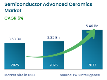
The global semiconductor advanced ceramics market size was valued at USD 3.63 billion in 2025 and is estimated at USD 3.85 billion in 2026. Revenue is projected to reach USD 5.46 billion by 2032, growing at a CAGR of 6.0% during 2026-2032. Chipmakers and equipment builders buy these parts because plasma, fluorine chemistry, and thermal cycling destroy metal and polymer hardware, so every chamber build and every chamber rebuild puts another order for rings, liners, chucks, and heaters on a supplier's books.
Spending tracks chip output more closely than chip prices. The Semiconductor Industry Association recorded global semiconductor sales of USD 791.7 billion in 2025, 25.6% above 2024, as AI accelerators and high-bandwidth memory pulled fabs toward full utilization. Erosion on a consumable ceramic part follows chamber hours, so heavy utilization shortens the interval between parts changes. For a qualified supplier, a customer's strong production year converts into repeat orders inside the same year, on top of the original tool sale.
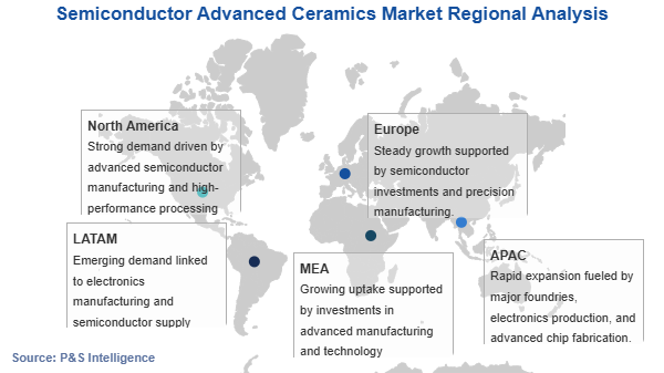
Asia-Pacific generated 46% of revenue in 2025, the largest share of any region, because most of the world's installed process chambers and most of its qualified parts machining are concentrated in China, Japan, South Korea, and India. The region also leads on growth, with semiconductor advanced ceramics demand projected to rise at a 7.0% CAGR over 2026-2032. Mature markets buy mainly replacement and refurbishment volume, while new memory, mature-node, and packaging capacity across Asia-Pacific still generates first-fill orders on newly installed tools. Suppliers with qualified local machining and refurbishment capacity are best placed to win that work.
Key Market Insights
By material type, alumina held 32% of the market in 2025, while silicon nitride is forecast to expand at an 8.1% CAGR over 2026-2032.
By application (equipment type), wafer processing equipment accounted for 49% of revenue in 2025, while assembly and packaging equipment is forecast to expand at a 7.2% CAGR over 2026-2032.
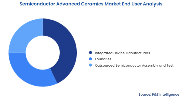
By end user, integrated device manufacturers held 43% of the market in 2025, while OSATs are forecast to expand at a 6.1% CAGR over 2026-2032.
By geography, Asia-Pacific generated 46% of revenue in 2025, and the region is forecast to expand fastest, at a 7.0% CAGR over 2026-2032.
Semiconductor Advanced Ceramics Market Trends and Growth Drivers
Rising Equipment Build Rates Are Redefining Consumable Ceramic Supply
Toolmakers are building etch and deposition chambers at a rising rate, and each chamber ships with a full ceramic set of rings, liners, gas distribution plates, and wafer supports before it reaches a fab. Parts suppliers therefore see the same installed chamber twice, once as first-fill content inside a new tool and again as replacement stock once that tool runs production wafers. The first stream follows tool build schedules, which move faster and change more often than fab construction plans.
The Semiconductor Equipment Association of Japan forecasts Japanese equipment sales of JPY 5.50 trillion in fiscal 2026, 12% above the prior year, on DRAM investment and advanced logic for AI servers. Japanese toolmakers supply a large share of etch, deposition, and thermal platforms, so their build plans set the order books of the ceramic suppliers qualified on those platforms. A supplier holding a qualified part number on a high-volume chamber captures both revenue streams. A capable machinist without that qualification captures neither, however competitive the quote.
Government-Backed Fab Construction Is Accelerating First-Fill Component Orders
Publicly funded fab projects have added buyers that did not exist five years ago. A new 300mm fab commissions hundreds of process chambers, and every chamber needs its ceramic set installed, leak-checked, and process-qualified before the first production wafer runs. That front-loads supplier revenue, because the first-fill order lands during tool installation, ahead of the ramp. Fabs also stock spare rings, chucks, and heaters on site before startup, which lifts the opening order well above steady-state replacement volumes.
The U.S. Government Accountability Office (GAO) reported that the Department of Commerce allocated $30.9 billion in direct funding across 40 projects at 19 companies, with subsequent updates showing expansion to 49 projects across 24 companies by mid-2026. Those awards commit construction spending, and the ceramic content arrives tool by tool as each project reaches installation. Suppliers with machining, cleaning, and coating operations close to those sites are better placed to win the qualification and spares work, because a fab will not wait weeks for a part that stops a chamber.
Power Device Lines Are Opening a Higher-Temperature Product Niche
Silicon carbide and gallium nitride device lines buy a different ceramic set from silicon logic fabs. High-temperature implant annealing and epitaxy run hotter than standard alumina hardware tolerates, which pushes those lines toward silicon carbide and aluminum nitride susceptors, trays, and heaters. Power device makers commissioning dedicated 150mm and 200mm lines specify those materials at the design stage, and few suppliers hold qualified positions in them today. That narrow qualified base is what makes the niche worth entering.
The International Energy Agency reported that electric car sales passed 20 million in 2025, a quarter of all cars sold worldwide. Traction inverters and onboard chargers in those vehicles increasingly use silicon carbide power devices, which supports sustained wafer starts on the lines that need high-temperature ceramic hardware. A demand base of that size gives a ceramic supplier a commercial reason to fund a second qualification path beyond silicon logic chambers.
Export Licensing on Rare Earth Feedstocks Is Constraining Coated Parts Supply
Plasma-facing parts often carry yttria or yttria-stabilized coatings, which places a rare earth feedstock inside an otherwise straightforward ceramic component. Licensing requirements on that feedstock lengthen quoted lead times and push suppliers to hold more inventory, and both raise the delivered cost of a coated ring or liner. Fabs cannot simply order the uncoated version, because coating life determines how often a chamber comes down for a parts change and therefore how much output the fab loses to maintenance.
China's Ministry of Commerce placed yttrium and six other medium and heavy rare earth items under per-shipment export licensing in April 2025, requiring end-user certificates and value-chain documentation for each consignment. The measure adds timing and paperwork to each shipment and leaves supply open, but it inserts an approval step ahead of a material with few alternative sources at scale. Buyers running single-source coated parts carry the greater exposure here, and suppliers that qualify a second coating chemistry or a second feedstock route reduce it.
Alumina held 32% of the Semiconductor Advanced Ceramics Market in 2025. It is the grade most fabs already have qualified, and that installed qualification matters more than marginal performance, because requalifying a chamber part costs test wafers, particle measurements, and tool time. Alumina also presses, sinters, and grinds at lower cost than nitride or carbide grades, so equipment designers specify it wherever plasma exposure and thermal load stay inside its limits. Chamber liners, insulators, and wafer-handling hardware account for much of that volume. For buyers, a second alumina source is the cheapest hedge available, since the qualification path already exists.
Silicon nitride is set to post the fastest growth of any material, at an 8.1% CAGR over 2026-2032. Its fracture toughness lets designers build thinner, lighter wafer-handling arms, rollers, and bearings that survive the acceleration faster tool throughput demands. The same toughness reduces edge chipping, which is a direct particle source in high-aspect-ratio etch. Suppliers able to sinter and finish large silicon nitride shapes to tight flatness hold the clearest opening, since grinding cost usually decides the quote more than powder cost does. Toolmakers that design them in early tend to keep one supplier through a platform's run.
Application (Equipment Type)
Wafer processing equipment represented 49% of revenue in 2025. Etch and deposition chambers carry the heaviest ceramic content of any tool class and consume it fastest, because fluorine and chlorine plasmas erode rings, liners, and gas distribution plates on a cycle measured in chamber hours. A single high-volume fab runs hundreds of these chambers, each coming down for a parts change several times a year. That rhythm makes wafer processing a recurring consumables business for suppliers, with revenue that continues after the tool sale. Suppliers that hold chamber-specific qualifications gain pricing leverage, since a fab cannot swap parts mid-recipe.
Assembly and packaging equipment is on course for the steepest CAGR of any equipment type, at 7.2% during 2026-2032. SEMI reports that assembly and packaging equipment sales rose 20.8% in 2025. The association projects USD 6.7 billion for 2026, supported by heterogeneous packaging and high-bandwidth memory. Bonders, reflow systems, and hybrid bonding platforms need precision ceramic stages, chucks, and heater plates that hold flatness through repeated thermal cycles, and orders follow tool installs closely. Suppliers already serving wafer-processing accounts can often run these parts on the same presses and grinders, which shortens their route into a new customer base.
End User
Integrated device manufacturers held 43% of the market in 2025. Memory and analog IDMs own both their fabs and their process recipes, so they qualify ceramic parts directly and often hold one specification across several fabs. That gives a qualified supplier a large repeating account and replaces a string of tool-by-tool wins. IDMs also carry deeper spares inventories, because an unplanned chamber outage costs them wafer output they cannot buy back from anyone else. Suppliers that already hold an IDM's specification can extend it to adjacent product lines with a shorter qualification, which keeps the account sticky.
OSATs are set to grow fastest among end users, at a 6.1% CAGR during 2026-2032, and their spending shows up plainly in equipment budgets. ASE Technology Holding reported equipment capital expenditure of USD 3,396 million for 2025, of which USD 2,104 million went to packaging operations, more than half of the total. Every new bonding and test line adds ceramic chucks, heater plates, and handling parts, and the parts count per line rises as package sizes grow. Short-run, high-mix machining suits this buyer better than volume production geared to a single ring design.
The complete segmentation hierarchy is as follows:
Material Type
Alumina
Aluminum Nitride
Silicon Nitride
Silicon Carbide
Zirconia
Others
Application (Equipment Type)
Wafer Processing Equipment
Assembly & Packaging Equipment
Testing Equipment
Others
End User
Integrated Device Manufacturers (IDMs)
Foundries
Outsourced Semiconductor Assembly and Test (OSATs)
Drive strategic growth with comprehensive market analysis
Asia-Pacific Semiconductor Advanced Ceramics Market Outlook
Asia-Pacific held 46% of the Semiconductor Advanced Ceramics Market in 2025. The region is also projected to grow fastest, at a 7.0% CAGR during 2026-2032. Most of the world's installed wafer-processing chambers operate in the region, so most ring, liner, and chuck replacements are bought there. Japan adds a second source of demand, because the suppliers qualified on many etch and deposition platforms press, machine, and coat those parts domestically. Korean memory fabs carry heavy chamber-hour loads, which lifts consumable spend per tool.
The National Bureau of Statistics of China reported integrated circuit output of 484.28 billion units in 2025, 10.9% above 2024. That figure counts device output and says nothing directly about parts spending, but chamber hours scale with wafer starts, and chamber hours are what set consumable replacement volumes. Regional growth should stay ahead of other regions while memory and mature-node capacity keeps coming online in China and while India's first fab and packaging projects move into production. Suppliers with local cleaning, recoating, and refurbishment operations capture service work that travels poorly across borders.
North American buyers contribute the second-largest block of demand, and their orders weight toward newly installed leading-edge capacity. Several publicly funded logic and memory fabs moved into installation and early production during 2025 and 2026, which compresses first-fill ceramic sets and startup spares into a short window. Equipment makers headquartered in the region also specify parts for tools they ship worldwide, so purchases recorded here partly cover chambers that will operate elsewhere. Fab operators in Arizona, Texas, Ohio, and New York are the accounts that matter most.
Innovation, Science and Economic Development Canada funds FABrIC, a five-year initiative of CAD 223 million covering domestic photonics, MEMS, and compound semiconductor capability. Programs of that size build pilot and small-volume lines, which generates demand for custom ceramic fixtures and susceptors and little repeat consumable volume. Suppliers that can quote single-piece and short-run work profitably fit this buyer, while those geared to standard ring production see little of it. Mexico's contribution runs through Latin America, where its plants concentrate on back-end assembly.
European demand comes mainly from power, analog, and sensor fabs rather than leading-edge logic, and that changes the ceramic mix a supplier needs to carry. Those fabs run more high-temperature thermal processing and more silicon carbide device work, so they buy proportionally more aluminum nitride and silicon carbide hardware and fewer advanced etch consumables. Germany, France, and Italy host most of that capacity. Regional ceramic suppliers sit close to those customers, which shortens qualification cycles and cuts the turnaround time on refurbishment and recoating orders.
The European Court of Auditors reported in 2025 that the European Union was on course for roughly 11.7% of global chip production by 2030, well short of its 20% target. Slower capacity addition means fewer first-fill orders and a demand pattern led by replacement at fabs already running. Suppliers in the region gain more from chasing the power and compound semiconductor specifications where European fabs actually invest than from waiting for leading-edge volume that may not arrive on the original timetable.
Latin America trails the leading regions, and the demand that exists comes from back-end assembly, test, and packaging rather than wafer fabrication. Mexico anchors that activity, with electronics plants clustered along the northern border and in central manufacturing states serving automotive and computing customers. Back-end tools consume ceramic chucks, heater plates, and handling parts, but far less plasma-exposed consumable content per tool than an etch chamber, so revenue per installed tool stays well below front-end levels.
The Organisation for Economic Co-operation and Development assessed Mexico's semiconductor sector and found its semiconductor activity concentrated in design and in assembly, testing, and packaging, with no front-end fabrication facilities. That positioning ties regional ceramic demand to packaging equipment installs and their spares. Suppliers already serving OSAT accounts in Asia can extend the same product range here without fresh qualification work, which makes the region a straightforward adjacency for an established supplier and a difficult standalone target for a new one.
The Middle East and Africa remain among the smallest sources of demand, because the region has very little installed wafer-processing capacity to maintain. Spending in Saudi Arabia and the United Arab Emirates goes mostly to design centers, research lines, and data center infrastructure, with few production fabs. South Africa's activity is smaller again and centered on university and research institute cleanrooms that buy a handful of parts at a time.
Saudi Arabia's National Semiconductor Hub aims to attract at least 50 semiconductor design companies by 2030, backed by a USD 266 million deep-tech fund. Design work buys software, tools, and engineers and few process chambers, so that program adds little near-term ceramic parts demand even as it raises the region's standing with equipment makers. Ceramic suppliers get more from tracking pilot line and packaging plant announcements here, since those are the projects that place hardware orders.
The regions and countries in scope are listed below.
The semiconductor advanced ceramics market is oligopolistic, with a few suppliers holding the qualified positions on most high-volume process chambers. Three barriers keep that group small. Qualification runs through the equipment maker and then the fab, and takes months of test wafers and particle data. Pressing, sintering, and precision grinding of large high-purity parts is capital intensive, with furnace and grinder spending committed years ahead of the revenue. Process recipes are also confidential, so a supplier that has tuned a part to one customer's chemistry is hard to displace. Each barrier takes years to build, so the structure lasts.
Kyocera Corporation and NGK Insulators Ltd. compete on breadth, covering electrostatic chucks, heaters, and structural parts across multiple materials, and both are adding capacity in Japan. TOTO Ltd. competes from a narrower base built on electrostatic chucks and precision structural components for etch chambers. CoorsTek Inc. sells from US and Japanese plants and competes on proximity to equipment makers in both markets. Ferrotec Holdings Corporation pairs ceramic parts with quartz, silicon parts, and contract machining, which lets it quote a larger portion of a chamber's consumable content in one package.
Competition turns less on list price than on lead time, particle performance, and the ability to hold one specification across multiple fabs. Fabs qualify a second source on critical parts to protect against an outage, which gives specialist suppliers a route into accounts they could not win outright. Refurbishment and recoating are becoming a second competitive front, because a supplier that restores a used part earns more revenue per component while giving the fab a cheaper option than buying new.
Leading Companies in the Semiconductor Advanced Ceramics Market:
In September 2026, Kyocera Corporation held the completion ceremony for its Nagasaki Isahaya Plant in Isahaya, Nagasaki Prefecture, a facility carrying roughly JPY 68 billion of investment through March 2029 and producing fine ceramic components for semiconductor manufacturing equipment alongside semiconductor packages. Phased production has begun, with full-scale operations scheduled for spring 2027, adding qualified capacity in Japan close to the company's equipment-maker customers.
In April 2026, NGK Insulators Ltd. approved a new production site in Nomi, Ishikawa Prefecture, investing about JPY 70.0 billion on roughly 104,000 square meters of adjacent land to build ceramic susceptors that support silicon wafers, with mass production set for October 2029. The plant is expected to raise group capacity for semiconductor equipment ceramics by about 20%, committing long-lead furnace and grinding capacity well ahead of the demand it serves.
Frequently Asked Questions About This Report
What drives demand for ceramic parts in semiconductor manufacturing?+
Plasma, fluorine chemistry, and thermal cycling destroy metal and polymer hardware, so every chamber build and every chamber rebuild puts another order for rings, liners, chucks, and heaters on a supplier's books.
How are ceramic components equipped on new semiconductor tools?+
Toolmakers are building etch and deposition chambers at a rising rate, and each chamber ships with a full ceramic set of rings, liners, gas distribution plates, and wafer supports before it reaches a fab.
Why do fabs prefer established ceramic materials?+
It is the grade most fabs already have qualified, and that installed qualification matters more than marginal performance, because requalifying a chamber part costs test wafers, particle measurements, and tool time.
What advantages does silicon nitride offer manufacturers?+
Suppliers able to sinter and finish large silicon nitride shapes to tight flatness hold the clearest opening, since grinding cost usually decides the quote more than powder cost does.
How often do high-volume fabs replace ceramic consumables?+
A single high-volume fab runs hundreds of these chambers, each coming down for a parts change several times a year.
How do integrated device manufacturers maintain supplier relationships?+
Memory and analog IDMs own both their fabs and their process recipes, so they qualify ceramic parts directly and often hold one specification across several fabs.
Want a report tailored exactly to your business need?
Leading companies across industries trust us to deliver data-driven insights and innovative solutions for their most critical decisions. From data-driven strategies to actionable insights, we empower the decision-makers who shape industries and define the future. From Fortune 500 companies to innovative startups, we are proud to partner with organisations that drive progress in their industries.
Client Testimonials
Working with P&S Intelligence and their team was an absolute pleasure – their awareness of timelines and commitment to value greatly contributed to our project's success. Eagerly anticipating future collaborations.
McKinsey & Company
India
Unmatched Standards
Our insights into the minutest levels of the markets, including the latest trends and competitive landscape, give you all the answers you need to take your business to new heights
Complete Data Security
We take a cautious approach to protecting your personal and confidential information. Trust is the strongest bond that connects us and our clients, and trust we build by complying with all international and domestic data protection and privacy laws