This Report Provides In-Depth Analysis of the Physical Vapor Deposition Market Report Prepared by P&S Intelligence, Segmented by Component (Equipment, Material, Service), Process (Sputter Deposition, Cathodic Arc Deposition, Electron Beam Deposition), Application (Microelectronics, Data Storage, Solar Products, Cutting Tools, Medical Equipment), and Geographical Outlook for the Period of 2021 to 2032
Explore the market potential with our data-driven report
Physical Vapor Deposition Market Overview
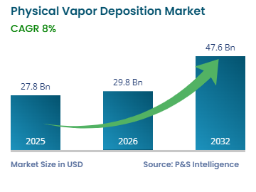
The physical vapor deposition market size was USD 27.8 billion for 2025, and it will grow by 8.0% during 2026–2032, to reach USD 47.6 billion by 2032.
This growth is supported by the expanding adoption of sputter deposition and cathodic arc deposition across microelectronics, solar products, cutting tools, and medical equipment manufacturing, making PVD a foundational thin-film deposition technology for semiconductor manufacturing and precision surface engineering.
The Semiconductor Industry Association (SIA) reports that global semiconductor sales reached USD 82.5 billion in January 2026, a 46.1% increase from January 2025. As integrated circuit designs become increasingly complex, PVD equipment is essential for depositing thin films on semiconductor wafers, sustaining demand for sputtering and evaporation systems. Rising adoption of thin-film solar cells is also accelerating PVD demand in photovoltaic manufacturing, while cutting-tool and medical-device applications continue to expand the use of cathodic arc coatings due to their superior hardness, wear resistance, and biocompatibility.
Key Market Insights
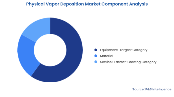
The equipment category holds the largest market share, of 60%, in 2025, driven by high PVD system costs and rising deployment.
The cathodic arc deposition is the fastest-growing category, of approximately 8.5%, driven by rising demand for durable, wear-resistant coatings across industrial and medical applications.
The microelectronics category holds the largest market share, of 35%, in 2025, driven by extensive PVD use in semiconductor manufacturing.
The solar products category will have the highest CAGR, of approximately 8.7%, driven by rising renewable energy investment and thin-film PV adoption.
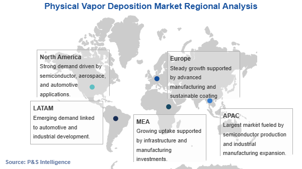
Asia-Pacific holds the largest market share, of 40%, in 2025, and it will have the highest CAGR, of approximately 8.9%, driven by strong semiconductor and electronics manufacturing.
Physical Vapor Deposition Market Trends and Drivers
Rising Investments in Advanced Semiconductor Fabrication Is Key Trend
The rapid expansion of advanced semiconductor fabrication facilities worldwide is accelerating demand for physical vapor deposition (PVD) technologies, as increasingly complex chip architectures require high-precision thin-film deposition for interconnects, barrier layers, and advanced packaging. Growing investments in AI, high-performance computing (HPC), and memory devices are driving the deployment of next-generation PVD equipment capable of delivering greater process precision and higher production throughput.
According to SEMI, global front-end semiconductor fab equipment spending is expected to reach USD 110 billion in 2025, marking the sixth consecutive year of growth since 2020, while spending is projected to increase to USD 130 billion in 2026 as manufacturers expand production capacity to meet AI-driven semiconductor demand. This sustained investment in wafer fabrication facilities is reinforcing long-term demand for PVD systems used across advanced semiconductor manufacturing.
Growing Demand for High-Performance and Wear-Resistant Coatings Is Biggest Driver
The increasing demand for high-performance, wear-resistant, and corrosion-resistant surface coatings across manufacturing industries is a major driver of the physical vapor deposition (PVD) market. PVD coatings significantly enhance the hardness, wear resistance, oxidation resistance, and service life of cutting tools, molds, dies, aerospace components, and medical devices, enabling manufacturers to improve productivity, reduce maintenance costs, and support high-speed machining. The growing adoption of precision manufacturing and difficult-to-machine materials, including titanium alloys and high-strength steels, is further accelerating the use of advanced PVD coating technologies.
The widespread adoption of coated cutting tools continues to reinforce demand for PVD technologies. According to a review published in the CIRP Journal of Manufacturing Science and Technology, approximately 85% of all cemented carbide cutting tools are now coated to improve machining performance and tool life. The increasing use of coated cutting tools reflects manufacturers' growing focus on extending tool life, improving machining efficiency, and reducing replacement and maintenance costs, thereby supporting continued demand for PVD coatings.
High Capital Investment and Complex Process Integration Are Key Restraints
The high capital investment required for physical vapor deposition (PVD) systems remains a major restraint to market growth. PVD equipment involves sophisticated vacuum chambers, plasma generation systems, precision deposition sources, and advanced process control technologies that require significant upfront expenditure. In addition to equipment costs, manufacturers must invest in cleanroom infrastructure, vacuum pumps, cooling systems, and skilled personnel to operate and maintain these highly specialized systems. These requirements can discourage adoption, particularly among small and medium-sized enterprises (SMEs) and manufacturers in cost-sensitive markets.
The complexity of integrating PVD systems into existing production lines further limits market expansion. Achieving consistent thin-film quality requires precise control over deposition parameters such as vacuum pressure, substrate temperature, coating thickness, and target material composition. Any deviation can affect coating performance, increase material wastage, and reduce production efficiency, necessitating continuous process optimization and regular equipment maintenance. Many manufacturers delay or limit investments in PVD technology despite its long-term performance benefits, particularly where production volumes or return on investment do not justify the high initial costs.
Expanding Adoption of Thin-Film Technologies in Next-Generation Energy and Electronics Is Biggest Opportunity
The expanding commercialization of next-generation thin-film technologies is creating substantial growth opportunities for the physical vapor deposition (PVD) market. Emerging applications such as tandem perovskite solar cells, flexible electronics, advanced displays, MEMS sensors, and solid-state batteries can require ultra-thin, high-uniformity functional coatings, creating opportunities for advanced PVD deposition technologies. As manufacturers focus on improving device efficiency, reducing material consumption, and enabling miniaturization, the demand for advanced sputtering and evaporation technologies is expected to increase across these high-value applications.
According to the International Energy Agency (IEA), perovskite technology now accounts for more than 70% of all solar cell patent families worldwide, highlighting its rapid technological advancement and commercialization potential. In addition, the IEA PVPS Trends Report 2025 states that experimental silicon-based tandem perovskite solar cells achieved a record efficiency of 34.6% in 2024, demonstrating the growing viability of next-generation thin-film photovoltaic technologies. As these advanced energy and electronics applications move toward large-scale commercialization, they are expected to create significant long-term opportunities for PVD equipment manufacturers supplying high-precision thin-film deposition solutions.
The equipment category holds the largest market share, of 60%, in 2025, due to the high capital value of PVD deposition systems and the increasing deployment of advanced sputtering, evaporation, and cathodic arc equipment across semiconductor fabrication, electronics, solar photovoltaic manufacturing, and precision industrial coating applications. According to SEMI's World Fab Forecast, global equipment spending is projected to reach USD 152 billion in 2026, representing a 24% year-over-year increase, driven by continued expansion of semiconductor fabrication facilities worldwide. Since PVD equipment is an essential part of wafer fabrication and thin-film deposition processes, sustained investments in new fabs continue to reinforce the dominance of the equipment segment.
The service category will have the highest CAGR, of approximately 8.4%, driven by the increasing installed base of PVD systems and the growing need for equipment maintenance, refurbishment, process optimization, calibration, and coating services. As manufacturers prioritize maximizing equipment uptime, improving coating quality, and extending system life while reducing operational costs, demand for specialized aftermarket and technical support services is expected to increase steadily across semiconductor, aerospace, automotive, and medical device industries.
The components analyzed in this report are:
Equipment (Largest Category)
Material
Service (Fastest-Growing Category)
Process Analysis
The sputter deposition category holds the largest market share, of 45%, in 2025, owing to its widespread use in semiconductor manufacturing, flat-panel displays, optical coatings, data storage devices, and thin-film solar cells. The process offers excellent film uniformity, precise thickness control, and compatibility with a wide range of metals, alloys, and ceramic materials, making it the preferred PVD technique for high-volume industrial production. According to SEMI, 300 mm semiconductor fab capacity is projected to reach a record 11.1 million wafers per month by the end of 2028, reflecting the continued expansion of advanced wafer fabrication facilities where sputter deposition is a critical thin-film deposition process.
The cathodic arc deposition category will have the highest CAGR, driven by increasing demand for ultra-hard, wear-resistant, and corrosion-resistant coatings across cutting tools, aerospace components, automotive parts, and medical implants. The process provides superior coating adhesion, high deposition rates, and dense film structures, making it particularly suitable for high-performance industrial applications. Growing adoption of advanced machining technologies and precision-engineered components is expected to further accelerate demand for cathodic arc deposition systems during the forecast period.
The microelectronics category holds the largest market share in 2025, driven by the extensive use of physical vapor deposition (PVD) in semiconductor wafer fabrication, integrated circuits, MEMS devices, sensors, and advanced packaging. PVD processes are essential for depositing conductive, dielectric, and barrier thin films with high precision, enabling the production of increasingly miniaturized and high-performance electronic devices. According to SEMI, worldwide silicon wafer shipments totaled 12,266 million square inches (MSI) in 2024, with demand beginning to recover during the second half of the year, supporting continued investment in semiconductor manufacturing and reinforcing demand for PVD technologies used in thin-film deposition.
The solar products category will have the highest CAGR, of approximately 8.7%, supported by expanding investments in renewable energy and the rapid adoption of thin-film photovoltaic technologies. PVD plays a critical role in depositing functional coatings for thin-film solar cells, improving energy conversion efficiency and device durability. According to the International Energy Agency (IEA), China added more than 340 GW of solar PV capacity in 2024, accounting for nearly two-thirds of global renewable capacity additions.
The applications analyzed in this report are:
Microelectronics (Largest Category)
Data Storage
Solar Products (Fastest-Growing Category)
Cutting Tools
Medical Equipment
Others
Drive strategic growth with comprehensive market analysis
Asia-Pacific holds the largest market share, of 40%, in 2025, and it will have the highest CAGR, of approximately 8.9%, supported by concentrated semiconductor manufacturing hubs across China, Japan, South Korea, and India, alongside expanding electronics production and solar panel manufacturing capacity. The region's integrated supply chains and sustained government investment in high-tech manufacturing continue to reinforce structural demand for PVD equipment across semiconductor fabrication, display panel production, photovoltaic manufacturing, and precision industrial coating applications.
According to the International Energy Agency (IEA), China added more than 340 GW of solar PV capacity in 2024, accounting for nearly two-thirds of global renewable capacity additions. This rapid expansion of solar PV capacity, combined with continued investments in semiconductor fabrication and advanced electronics production, is accelerating demand for physical vapor deposition technologies used in thin-film deposition for solar cells, semiconductor devices, and display components.
India Physical Vapor Deposition Market Size
India is projected to be among the fastest-growing country markets within Asia-Pacific, driven by an accelerating national push toward domestic semiconductor manufacturing and electronics production. Government-backed investments in semiconductor fabrication, assembly, testing, marking, and packaging (ATMP), and chip design are creating new demand for thin-film deposition equipment, supporting India's transition from component assembly to advanced semiconductor manufacturing.
According to the Press Information Bureau (PIB), Government of India, the domestic semiconductor market was valued at approximately USD 38 billion in 2023 and is projected to reach USD 100–110 billion by 2030, supported by the India Semiconductor Mission's INR 76,000 crore incentive program for semiconductor fabrication, packaging, and chip design. The expansion of domestic semiconductor manufacturing capacity is expected to accelerate demand for physical vapor deposition equipment used in thin-film deposition, wafer processing, and advanced microelectronics production.
North America Physical Vapor Deposition Market Size
North America accounted for a significant share of the global PVD market in 2025, driven by advanced semiconductor manufacturing and research capabilities, a concentrated base of precision-coating technology providers, and strong adoption of PVD in aerospace and medical device manufacturing. The region benefits from continuous innovation in sputtering and evaporation systems, alongside rising investment in domestic chip fabrication and clean-energy manufacturing, reinforcing demand for thin-film coating equipment.
The U.S. has been especially influential in shaping regional PVD adoption due to its leadership in semiconductor manufacturing, fabrication equipment, and advanced materials innovation. The CHIPS and Science Act provides USD 39 billion in incentives for semiconductor manufacturing and USD 11 billion for semiconductor research and development, accelerating investments in advanced wafer fabrication facilities across the U.S. These investments are strengthening domestic semiconductor production capacity and increasing demand for PVD equipment used in thin-film deposition, advanced chip manufacturing, and precision coating applications.
The regions and countries analyzed in this report are:
North America
U.S. (Larger Country)
Canada (Faster-Growing Country)
Europe
Germany (Largest Country)
U.K. (Fastest-Growing Country)
France
Italy
Spain
Rest of Europe
Asia-Pacific (Largest and Fastest-Growing Regional Market)
The market is fragmented, with competition led by established global equipment manufacturers and coating specialists, while numerous regional and niche players serve application-specific and local markets. Leading companies compete through continuous technological innovation, product portfolio expansion, strategic partnerships, and investments in advanced sputtering, evaporation, and coating technologies. Meanwhile, specialized providers differentiate themselves by offering customized PVD systems and coating services for industries such as semiconductors, aerospace, medical devices, cutting tools, and renewable energy.
Major companies, including Applied Materials, Inc., Lam Research Corporation, Veeco Instruments Inc., Oerlikon Balzers, and IHI Corporation, continue to strengthen their market positions through investments in next-generation PVD equipment, strategic collaborations, product innovation, and capacity expansion. At the same time, regional and niche manufacturers remain competitive by providing customized coating solutions and application-specific deposition systems tailored to local customer requirements. The diverse end-use applications of PVD technologies and the rapid pace of technological advancement continue to create opportunities for both global leaders and specialized regional players to expand their presence in the market.
Key Players in the Physical Vapor Deposition Market:
Oerlikon Balzers
ULVAC, Inc.
Applied Materials, Inc.
Veeco Instruments Inc.
IHI Hauzer Techno Coating B.V.
Angstrom Engineering Inc.
Kurt J. Lesker Company
Denton Vacuum LLC
Vapor Technologies, Inc.
AJA International, Inc.
PLATIT AG
PVD Products, Inc.
Lam Research Corporation
Physical Vapor Deposition Market Developments
In November 2025, Oerlikon Balzers introduced INSPIRA carbon, a new coating platform integrating its S3p Technology for precision components and tooling applications. The launch expands Oerlikon's advanced surface-solutions portfolio serving aerospace, automotive, and medical device manufacturers.
In February 2025, ULVAC, Inc. developed the EWL-030, a roll-to-roll deposition system for lithium coating applications, scheduled for launch in May 2025. The system applies ULVAC's thin-film deposition expertise to next-generation battery manufacturing, supporting global electric vehicle battery production scale-up.
In May 2025, Vapor Technologies, Inc. announced the V.MAX1500 PVD and DLC flexible coating system, featuring up to six cathodic arc and/or magnetron sputtering sources for industrial coating applications. The system is designed for cutting and forming tools, precision components, automotive and aerospace parts, medical devices, and other functional components.
Frequently Asked Questions About This Report
What are the key benefits of Physical Vapor Deposition coatings?+
PVD coatings provide high hardness, wear resistance, corrosion protection, improved surface performance, and longer component life while enabling thin and uniform coatings.
What are the major challenges facing the Physical Vapor Deposition market?+
High initial equipment costs, complex process requirements, skilled-labor requirements, maintenance needs, and competition from alternative coating technologies are major challenges for the market.
How is PVD technology used in semiconductor manufacturing?+
PVD is used to deposit thin metal and other material films onto semiconductor wafers for applications such as metallization, barrier layers, and interconnect structures.
What technological developments are shaping the Physical Vapor Deposition market?+
Advancements in sputtering, cathodic arc deposition, high-power impulse magnetron sputtering, automation, process monitoring, and development of advanced coating materials are shaping the market.
What opportunities exist for PVD equipment manufacturers?+
Growing semiconductor manufacturing, expansion of electric vehicles and renewable-energy technologies, increasing demand for coated cutting tools, and adoption of high-performance coatings in aerospace and medical applications are creating opportunities for PVD equipment manufacturers.
Want a report tailored exactly to your business need?
Leading companies across industries trust us to deliver data-driven insights and innovative solutions for their most critical decisions. From data-driven strategies to actionable insights, we empower the decision-makers who shape industries and define the future. From Fortune 500 companies to innovative startups, we are proud to partner with organisations that drive progress in their industries.
Client Testimonials
Working with P&S Intelligence and their team was an absolute pleasure – their awareness of timelines and commitment to value greatly contributed to our project's success. Eagerly anticipating future collaborations.
McKinsey & Company
India
Unmatched Standards
Our insights into the minutest levels of the markets, including the latest trends and competitive landscape, give you all the answers you need to take your business to new heights
Complete Data Security
We take a cautious approach to protecting your personal and confidential information. Trust is the strongest bond that connects us and our clients, and trust we build by complying with all international and domestic data protection and privacy laws