India Semiconductor Materials Market Size & Share Analysis - Emerging Trends, Growth Opportunities, Competitive Landscape, and Forecasts (2026 - 2032)
This Report Provides In-Depth Analysis of the India Semiconductor Materials Market Report Prepared by P&S Intelligence, Segmented by Copper–Indium–Gallium Selenide, Application (Fabrication, Packaging), Device Type (Memory Devices, Logic Devices, ICs, Discrete Power Devices, MCUs, Sensors), End User (IDMs, Foundries, OSAT Companies, Fabless Companies), and Geographical Outlook for the Period of 2019 to 2032
India Semiconductor Materials Market Revenue Insights
Key Highlights
Study Period
2019 - 2032
Market Size in 2025
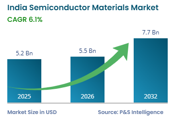
USD 5.2 Billion
Market Size in 2026
USD 5.5 Billion
Market Size by 2032
USD 7.7 Billion
Projected CAGR
6.1%
Largest State
Gujarat
Fastest-Growing State
Karnataka
Market Structure
Moderately Fragmented
Market Size
Explore the market potential with our data-driven report
India Semiconductor Materials Market Future Outlook
The Indian semiconductor materials market is valued at USD 5.2 billion in 2025, and it is projected to grow at a CAGR of 6.1% during 2026–2032, reaching USD 7.7 billion by 2032. The market expansion is driven by rising domestic semiconductor fabrication investments, increasing electronics manufacturing under the Production Linked Incentive scheme, and growing demand from consumer electronics and automotive sectors requiring specialized materials.
India's semiconductor materials sector is witnessing transformative growth as the country positions itself as a strategic player in the global chip supply chain. The India Semiconductor Mission has approved 10 major projects across six states with total investments exceeding INR 1.6 lakh crore, creating significant demand for silicon wafers, electronic gases, photoresists, and packaging materials. The National Policy on Electronics seeks to establish India as a worldwide center for electronics system design and manufacturing and generate USD 400 billion in revenue by 2025. This will substantially increase the consumption of semiconductor-grade materials across fabrication and assembly operations.
The government's PLI scheme allocation of INR 76,000 crore for semiconductor manufacturing is catalyzing material demand, with state-level incentives from Gujarat, Karnataka, and Tamil Nadu further accelerating ecosystem development. Micron Technology's operational USD 2.75-billion ATMP facility in Gujarat and Tata Electronics' upcoming USD 11-billion fabrication plant in Dholera exemplify the scale of investments driving material consumption. The growing adoption of IoT-enabled devices, with India's IoT market expected to reach USD 49.82 billion by 2029, is creating sustained demand for high-purity silicon wafers, specialty gases, and advanced packaging materials essential for smart electronics manufacturing.
India Semiconductor Materials Market Emerging Trends
Rising Consumer Electronics Production Is Driving Market Growth
India's consumer electronics market is growing rapidly due to smartphone penetration, IoT device adoption, and home automation trends.
According to the IBEF, India's smartphone production reached USD 49.55 billion in value in FY24, reflecting a rising need for high-purity materials for fabricating advanced semiconductor components.
As per the Press Information Bureau, smartphone penetration in India reached 85.5% of the households in 2024, driving the demand for connected devices, creating sustained requirements for silicon wafers, photoresists, and electronic gases used in chip fabrication.
The Make in India initiative has boosted local electronics manufacturing, with approximately 99.2% of smartphones sold in India now manufactured domestically, compared to merely 26% in 2014–15.
This localization trend extends to semiconductor materials, as manufacturers seek to reduce supply chain vulnerabilities and transportation costs.
The growing middle class, projected to reach 38% of India's population by 2031, is fueling consumption of consumer electronics including televisions, washing machines, and smart appliances, all of which require semiconductor chips manufactured with specialized materials.
Electric vehicle adoption is creating additional demand for power semiconductors and associated materials.
The government's ambitious target of 30% EV penetration by 2030 necessitates substantial semiconductor content, as modern EVs require 20–30% more semiconductor components than conventional vehicles.
This will substantially raise the requirement for silicon carbide wafers, wide-band-gap materials, and advanced packaging substrates for power management ICs and automotive-grade microcontrollers.
Automotive semiconductor requirements are driving investments in specialized materials that can withstand high temperatures and voltages.
Government Support for Local Semiconductor Production Offers Opportunities
The establishment of the India Semiconductor Mission as the nodal agency under the Ministry of Electronics and Information Technology has created a structured framework for semiconductor materials procurement and localization.
The government's commitment of INR 76,000 crore through the PLI scheme, with nearly INR 65,000 crore already allocated to approved projects, is directly stimulating demand for fabrication and packaging materials.
The scheme provides 50% fiscal support for capital expenditure on semiconductor fabs, compound semiconductor facilities, and ATMP units, making India an attractive destination for material suppliers seeking to establish local manufacturing capabilities.
State governments are complementing central incentives with dedicated semiconductor policies.
Gujarat's semiconductor policy, the first of its kind in India, offers land subsidies, infrastructure support, and capital incentives for projects in Dholera Special Investment Region and Sanand.
Karnataka, Tamil Nadu, Uttar Pradesh, and other states have introduced similar frameworks, creating geographically distributed demand centers for semiconductor materials.
The Electronics Component Manufacturing Scheme, announced in May 2025 with an outlay of INR 22,919 crore, aims to increase domestic value addition to 35% by 2030, necessitating localized supply of specialty chemicals, gases, and substrates.
This policy push is encouraging global material suppliers to establish manufacturing and distribution operations in India, reducing import dependency and transportation costs for semiconductor fabs.
India Semiconductor Materials Market Segmentation Analysis
Material Insights
Silicon holds the largest share, of approximately 35%, in the Indian semiconductor materials market in 2025, due to its established role as the fundamental substrate for most integrated circuits and its cost-effectiveness. Silicon wafers serve as the base for memory devices, logic chips, and analog circuits used extensively in consumer electronics, telecommunications infrastructure, and industrial applications.
Silicon carbide is experiencing the fastest growth during the forecast period, driven by the burgeoning electric vehicle adoption and renewable energy applications requiring power electronics that can operate at higher temperatures and voltages. The material's superior thermal conductivity and breakdown voltage make it ideal for EV inverters and solar inverters. RIR Power Electronics' August 2025 announcement to establish India's first Silicon Carbide semiconductor plant in Odisha to produce epitaxy wafers by December 2025 highlights the material's strategic importance for India's transition to clean energy and electric mobility.
These materials are covered:
Silicon (Largest Category)
Silicon Carbide (Fastest-Growing Category)
Gallium Arsenide
Germanium
Gallium Nitride
Copper–Indium–Gallium Selenide
Others
Application Insights
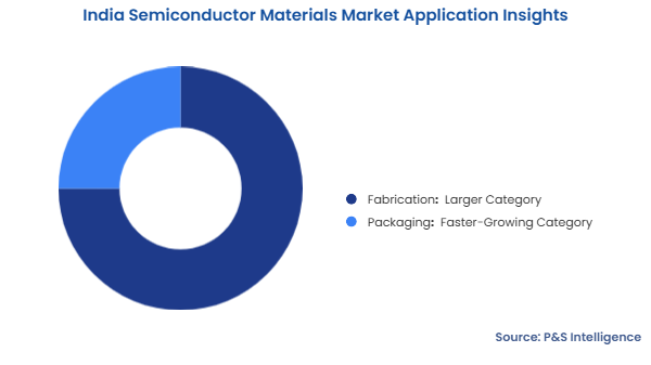
The fabrication category held the larger share, of approximately 75% in 2025, driven by the establishment of multiple semiconductor fabs requiring continuous supply of silicon wafers, electronic gases, photoresists, wet chemicals, CMP materials, and photomasks. Fabrication materials are consumed in larger volumes as they are essential for every stage of chip manufacturing from wafer preparation through photolithography, deposition, etching, and planarization. The operationalization of Tata Electronics' fab in Gujarat and other upcoming facilities is significantly expanding fabrication materials demand.
Packaging is witnessing the faster growth as India strengthens its position in assembly, testing, marking, and packaging operations. The category includes lead frames, organic substrates, ceramic packages, encapsulation resins, bonding wires, and die-attach materials used in converting fabricated wafers into finished semiconductor packages. Micron's operational ATMP facility and multiple OSAT projects approved under the India Semiconductor Mission are driving packaging materials consumption, particularly for advanced packaging technologies required for AI accelerators and high-performance computing applications.
These applications are covered:
Fabrication (Larger Category)
Packaging (Faster-Growing Category)
Device Type Analysis
Memory devices hold the largest share, of approximately 35%, in 2025, driven by massive production volumes of DRAM and NAND flash chips required for smartphones, data centers, and consumer electronics. The dominance of memory devices creates sustained demand for ultra-pure silicon wafers, specialty photoresists optimized for 3D NAND architectures, electronic gases including nitrogen and argon for deposition processes, and advanced CMP slurries for planarization of multiple memory layers. Micron Technology's operational ATMP facility in Gujarat manufactures DRAM and NAND memory packages, consuming significant volumes of organic substrates, bonding wires, encapsulation resins, and die-attach materials.
Logic devices are experiencing the fastest growth during the forecast period, propelled by increasing fabrication of microprocessors, ASICs, and FPGAs for telecommunications, automotive electronics, and AI acceleration applications. The establishment of logic fabrication capabilities through Tata Electronics' USD 11-billion fab in Dholera is creating substantial new demand for logic-optimized materials. According to the India Semiconductor Mission, the three semiconductor facilities expected to commence production in early 2026 will primarily focus on logic device manufacturing, significantly expanding materials consumption.
The growing deployment of 5G infrastructure is driving demand for ASICs, FPGAs, and RF logic devices requiring specialized materials. India's locally developed Shakti RISC-V microprocessor for IoT and edge computing applications demonstrates the country's expanding logic device design and manufacturing capabilities. The automotive sector's shift toward electric vehicles and ADAS is further accelerating logic device materials demand, particularly for power semiconductors manufactured using silicon carbide and gallium nitride substrates.
These device types are covered:
Memory Devices (Largest Category)
Logic Devices (Fastest-Growing Category)
Integrated Circuits
Discrete Power Devices
Microcontroller Units (MCUs)
Environmental Sensors
Others
End User Analysis
Integrated device manufacturers (IDMs) hold the largest share, of approximately 45%, in 2025, as these vertically integrated companies operate both fabrication facilities and packaging operations, requiring comprehensive materials supply across the semiconductor value chain. Tata Electronics is one of India's first major domestic IDMs, with its Dholera fab and Assam OSAT facility. IDMs consume the full spectrum of semiconductor materials from silicon wafers and fabrication chemicals for front-end manufacturing to packaging substrates and bonding wires for back-end assembly. Major global IDMs, including Intel, Samsung, and Micron Technology, operate design centers, testing facilities, and manufacturing plants in India, creating established procurement channels for semiconductor-grade materials.
OSAT companies are experiencing the fastest growth during the forecast period, driven by the operationalization of multiple assembly, testing, and packaging facilities under the India Semiconductor Mission. Micron Technology's fully operational ATMP facility in Gujarat, CG Power's partnership with Renesas Electronics for OSAT operations, and Tata Semiconductor Assembly and Test's facility in Assam collectively represent over USD 5 billion in packaging infrastructure investments. These facilities require continuous supply of packaging-specific materials including lead frames, organic substrates, ceramic packages, encapsulation resins, bonding wires, and die-attach materials.
The OSAT category's rapid expansion is supported by India's strategic positioning as a trusted assembly and testing hub in the global semiconductor supply chain. The shift toward advanced packaging technologies including 3D stacking, system-in-package solutions, and chiplet architectures is driving the demand for specialized materials supporting high-density interconnects and thermal management. Kaynes Semicon's achievement of first commercial shipment from its Sanand OSAT facility in October 2025 demonstrates the segment's operational maturity and materials consumption readiness.
These end users are covered:
IDMs (Largest Category)
OSAT Companies (Fastest-Growing Category)
Foundries
Fabless Companies
Drive strategic growth with comprehensive market analysis
India Semiconductor Materials Market Geographical Analysis
Gujarat Semiconductor Materials Market Demand
Gujarat holds the largest share, of approximately 40%, in the Indian semiconductor materials market in 2025, establishing itself as the primary consumption hub due to concentration of major semiconductor projects. The state hosts Micron Technology's operational USD 2.75 billion ATMP facility in Sanand, Tata Electronics' upcoming USD 11 billion fabrication plant in Dholera, and multiple OSAT facilities from CG Power and Kaynes. These projects collectively represent investments exceeding INR 1.5 lakh crore and require continuous supply of silicon wafers, electronic gases, photoresists, packaging substrates, and specialty chemicals.
The Dholera Special Investment Region, spanning 900 square kilometers with proximity to major ports, provides logistical advantages for materials procurement and distribution. Gujarat's dedicated semiconductor policy offers fiscal incentives, land subsidies, and infrastructure support, attracting global materials suppliers to establish local operations. According to industry sources, the state government is constructing 1,500 residential units to house fab workforces, indicating the scale of operational requirements including materials supply chains.
Gujarat's established industrial base in chemicals and gases provides foundational capabilities for semiconductor-grade materials production. The state's proactive approach in courting investments through single-window clearances and coordinated central-state incentive stacking has positioned it as India's semiconductor materials epicenter, with demand expected to grow substantially as fabrication facilities ramp production.
Karnataka Semiconductor Materials Market Growth
Karnataka is experiencing the fastest growth, with a CAGR of approx. 6.5%, during 2026–2032, leveraging Bengaluru's position as India's technology capital with concentration of R&D centers, design houses, and semiconductor startups. The state houses over 200 captive design centers operated by multinationals including Intel, AMD, and Qualcomm, employing approximately 125,000 chip design engineers who drive demand for prototyping materials and testing substrates.
Tata Electronics operates facilities in Karnataka employing over 15,000 people, with operations spanning electronics manufacturing services and semiconductor design. According to industry reports, AMD invested USD 400 million to establish its largest global design center in Bengaluru, while Lam Research committed over USD 1 billion for semiconductor tool engineering and training programs in the state. These investments create demand for advanced materials used in process development, failure analysis, and quality control.
Karnataka's focus on electric mobility is driving power semiconductor demand, with multiple EV manufacturers establishing operations requiring silicon carbide and gallium nitride materials for power electronics. The state's established engineering talent pool from institutions including Indian Institute of Science provides skilled workforce for materials characterization and quality assurance critical for semiconductor-grade materials supply.
These states are covered:
Gujarat (Largest State Market)
Karnataka (Fastest-Growing State Market)
Tamil Nadu
Maharashtra
Telangana
Uttar Pradesh
Rest of India
India Semiconductor Materials Market Share
The Indian semiconductor materials market is slightly fragmented with global materials suppliers dominating specialty chemicals, gases, and wafer supply while Indian companies are emerging in packaging materials and ancillary products. The market structure reflects the specialized nature of semiconductor-grade materials requiring strict purity standards, advanced manufacturing processes, and global certification, creating barriers to entry for new players.
Major global suppliers including DuPont, Merck, Shin-Etsu Chemical, Air Liquide, Linde, and Applied Materials have established or are expanding operations in India to serve growing fab and ATMP requirements. These companies leverage decades of materials science expertise, patented formulations, and integrated supply chains to maintain market positions. Local players including Tata Chemicals are developing capabilities in specialty chemicals and gases to serve the expanding domestic semiconductor industry.
Key India Semiconductor Materials Companies:
DuPont de Nemours Inc.
Merck KGaA
Shin-Etsu Chemical Co. Ltd.
Tokyo Ohka Kogyo Co. Ltd.
Air Liquide S.A.
Linde plc
Entegris Inc.
Chemours Company
Sumitomo Chemical Co. Ltd.
JSR Corporation
Fujifilm Corporation
BASF SE
Dow Inc.
Avantor Inc.
India Semiconductor Materials Market News
In June 2025, Micron Technology's Sanand, Gujarat plant achieved clean-room validation following USD 825 million first-phase investment, marking operational readiness for high-volume assembly and testing of advanced memory and storage solutions for global markets.
In May 2025, The Indian government approved INR 37.06 billion for HCL-Foxconn joint venture semiconductor fabrication plant near Jewar Airport, Uttar Pradesh, to manufacture 36 million display driver chips monthly with commercial production targeted for 2027 under the India Semiconductor Mission.
In January 2025, Indichip Semiconductors partnered with Japan's Yitoa Micro Technology to establish India's first private silicon carbide wafer fab in Kurnool, Andhra Pradesh, with INR 14,000 crore investment, scaling from 10,000 to 50,000 wafers monthly within three years to support EV and renewable energy sectors.
In September 2024, Tata Electronics signed an agreement with the India Semiconductor Mission to establish a semiconductor fabrication plant in Dholera, Gujarat, with INR 910 billion investment, partnering with Powerchip for technology transfer and targeting 50,000 wafers per month capacity for global automotive, AI, computing, and communication markets.
Want a report tailored exactly to your business need?
Leading companies across industries trust us to deliver data-driven insights and innovative solutions for their most critical decisions. From data-driven strategies to actionable insights, we empower the decision-makers who shape industries and define the future. From Fortune 500 companies to innovative startups, we are proud to partner with organisations that drive progress in their industries.
Client Testimonials
Working with P&S Intelligence and their team was an absolute pleasure – their awareness of timelines and commitment to value greatly contributed to our project's success. Eagerly anticipating future collaborations.
McKinsey & Company
India
Unmatched Standards
Our insights into the minutest levels of the markets, including the latest trends and competitive landscape, give you all the answers you need to take your business to new heights
Complete Data Security
We take a cautious approach to protecting your personal and confidential information. Trust is the strongest bond that connects us and our clients, and trust we build by complying with all international and domestic data protection and privacy laws