Explore the market potential with our data-driven report
Extreme Ultraviolet (EUV) Lithography Market Outlook
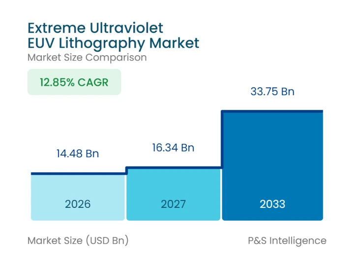
The global Extreme ultraviolet (EUV) lithography market size is estimated at USD 14.48 Billion in 2026 and is projected to reach USD 16.34 Billion in 2027. By 2033, revenue is projected to climb to USD 33.75 Billion, advancing at a CAGR of 12.85% during 2027-2033. Spending comes from a short list of leading-edge logic and DRAM manufacturers that need EUV exposure at each new node, because printing the densest layers with immersion multi-patterning adds process steps, mask sets, and yield risk. Each scanner order is tied to a specific fab ramp, so revenue concentrates in a few accounts.
Foundry customers designing AI accelerators and flagship mobile processors are moving production onto gate-all-around logic nodes, and each step down in pitch typically adds EUV exposures to the wafer flow. The largest contract foundry started volume production of its 2nm node in the fourth quarter of 2025 as planned and has scheduled an enhanced 2nm variant for the second half of 2026. Back-to-back node ramps keep scanner deliveries, light-source upgrades, and service contracts coming to the fabs that run them. Equipment revenue therefore follows foundry capacity plans closely.
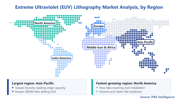
Asia-Pacific accounts for 71.2% of extreme ultraviolet (EUV) lithography revenue in 2026, because Taiwan, South Korea, and Japan host most of the fabs running EUV layers for logic and DRAM. Spending there leans on capacity additions, upgrades, and service for a large installed base. North America is projected to post a 14.5% CAGR during 2027-2033, the quickest of any region, as leading-edge logic and memory fabs in Arizona, Oregon, and Idaho move from construction to tool installation. Asian revenue is therefore weighted toward the installed base, while North American revenue arrives largely as first-time system deliveries.
Key market insights
By technology generation, 0.33 NA Low-NA EUV systems account for 68.5% in 2026, while 0.55 NA High-NA EUV systems are projected to advance at a 24.8% CAGR during 2027-2033.
By component and subsystem offering, EUV lithography scanners (complete systems) account for 58.0% in 2026, while optical subsystems & reflective optics are projected to grow at a 14.2% CAGR during 2027-2033.
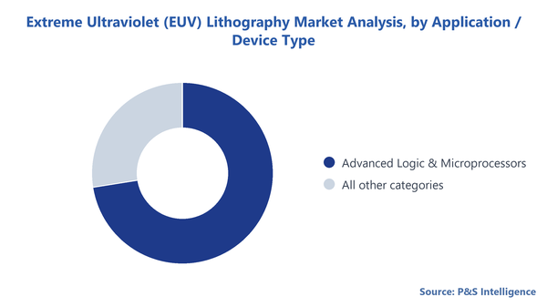
By application, advanced logic & microprocessors account for 72.5% in 2026, while advanced DRAM memory is projected to expand at a 16.5% CAGR during 2027-2033.
By end user, integrated device manufacturers (IDMs) account for 53.0% in 2026, while pure-play foundries are projected to post a 13.8% CAGR during 2027-2033.
By geography, Asia-Pacific accounts for 71.2% in 2026, while North America is projected to record a 14.5% CAGR during 2027-2033.
Rising light-source power is redefining reticle protection and resist specifications
Chipmakers running EUV scanners at higher source power are changing what they buy for masks and wafers. More power raises wafer output per tool, but it also raises the heat load on the pellicle that shields the reticle and shifts the dose window a photoresist must handle. Pellicles and resists are bought per mask and per wafer, so a specification change forces fabs to requalify materials layer by layer. Materials makers with membranes and resists already proven at the newest power levels are better positioned when those qualification slots open.
Mitsui Chemicals announced plans to build carbon nanotube pellicle production at its Iwakuni-Ohtake Works with capacity of 5,000 sheets per year, targeting EUV transmittance of 92% or above and light resistance for exposure output above 1kW, for High-NA and high-output tools rated at 600W or above. Construction was tentatively scheduled to end in December 2025. New membrane types are likely to enter high-power layers first, because fabs are reluctant to swap a protection material on a running production layer. That sequencing gives early-qualified producers recurring per-mask volumes that later entrants find hard to displace.
High-bandwidth memory demand is propelling EUV adoption in DRAM fabs
DRAM makers supplying AI servers are moving more layers of DDR5, LPDDR5X, and high-bandwidth memory base dies onto EUV as cell pitches tighten with each generation. Memory fabs run very high wafer volumes, so each EUV layer added to a DRAM node translates into a sizable block of scanner capacity, along with pellicles, masks, and resist. High-bandwidth memory stacks several DRAM dies in one package, which raises wafer starts at the newest nodes for every accelerator shipped.
According to SK hynix, the company has used EUV in advanced DRAM since 2021, starting with its 1a node, and in September 2025 it assembled an ASML TWINSCAN EXE:5200B High-NA system at its M16 fab in Icheon, which the company described as the industry's first High-NA tool for mass production. Memory makers that once trailed logic in EUV use are now ordering across both aperture generations. That widens the scanner customer base beyond the largest foundries and gives memory capital budgets more weight in delivery schedules.
Patterning limits below 2nm are opening a High-NA equipment cycle
Logic makers planning nodes beyond 2nm must choose between adding more Low-NA multi-patterning passes and moving critical layers to 0.55 NA High-NA scanners, which print finer features in a single exposure. Each High-NA system sells at a premium to earlier EUV platforms, so even a small number of orders lifts system revenue disproportionately. Each installation also creates demand for masks drawn for anamorphic optics, matching metrology, and long-term service contracts that sit outside the scanner sale itself.
As per Intel, the company completed assembly of the first commercial High-NA EUV system, an ASML TWINSCAN EXE:5000, at its Hillsboro, Oregon research site in April 2024, and it expects to use 0.33 NA and 0.55 NA EUV together as it moves into Intel 14A production. Mixed-aperture fabs of this kind point to a staged adoption path in which High-NA handles the tightest layers while Low-NA keeps the rest. Mask, inspection, and resist suppliers that qualify on High-NA flows early could secure a position in the next node cycle.
Export licensing requirements are limiting the addressable fab base
Export licensing has kept leading-edge fabs in China outside the EUV customer base, so scanner orders come from chipmakers in Taiwan, South Korea, Japan, the U.S., and Europe. The restriction removes a large pool of potential capacity from the market and leaves revenue dependent on the capital budgets of a handful of companies. A pause at one large customer therefore moves system revenue far more than it would in a broader equipment category, which raises earnings volatility for the scanner maker and its subsystem partners.
Under the EU dual-use export control regulation, step-and-scan lithography equipment with a light-source wavelength shorter than 193 nm is a listed item, which places every EUV scanner exported from the EU under the authorization regime. Approval depends on the destination and the end user, so licensing outcomes, as well as fab demand, decide which projects can add EUV capacity. If controls were widened to cover service and upgrades on installed tools, the recurring revenue base would narrow as well.
Segmentation Analysis
Technology Generation
0.33 NA Low-NA EUV systems account for 68.5% of Extreme ultraviolet (EUV) lithography revenue in 2026, because every chipmaker running EUV in volume does so on this platform. Low-NA recipes are already qualified at 3nm-class logic and current DRAM nodes, so new capacity repeats a proven process instead of opening a fresh qualification program. ASML specifications put NXE:3800E throughput at 220 wafers per hour at a 30 mJ/cm2 dose, against 160 on the NXE:3600D. Higher output per tool lowers exposure cost per layer, which keeps Low-NA units the default purchase for each new fab phase.
0.55 NA High-NA EUV systems are projected to expand at a 24.8% CAGR during 2027-2033, the quickest pace on this axis. The first production-grade units are moving from pilot use into logic and DRAM fabs, so annual unit volumes rise from a very low base. Higher selling prices than Low-NA units also raise the revenue booked per High-NA shipment. Fabs that adopt High-NA for the tightest layers can drop double-patterning steps on those layers, an argument that strengthens as pitches shrink toward 2nm-class rules and below.
Component and Subsystem Offering
EUV lithography scanners (complete systems) account for 58.0% of revenue in 2026. Only one company sells finished EUV scanners, and fabs book each unit as a multi-year asset, ordering several per fab phase before the first wafers run. This category counts the system maker's own value, while mirror sets, illumination optics, and drive lasers bought from subsystem partners are counted in their own categories, so the same hardware is not counted twice. For optics and laser makers, most volume reaches fabs through the scanner maker's order book, which ties their revenue to its delivery schedule.
Optical subsystems & reflective optics are projected to grow at a 14.2% CAGR during 2027-2033. Per Carl Zeiss SMT, a High-NA mirror is about twice as large and ten times as heavy as a current EUV mirror, and High-NA mirrors take around a year to manufacture. Larger mirror sets with year-long production cycles raise optics value per system as High-NA units take a growing share of shipments. Optics production lead times are therefore likely to influence how fast High-NA deliveries can scale.
Application
Advanced logic & microprocessors account for 72.5% of revenue in 2026. Leading-edge logic was the first production use of EUV, and gate-all-around processors for AI accelerators, servers, and smartphones typically carry more EUV layers per wafer than current DRAM. Foundries and logic manufacturers also add capacity in large fab phases timed to customer tape-outs, which concentrates scanner orders around a few node launches each year. For toolmakers, logic roadmaps set most of the near-term delivery schedule and the timing of light-source and throughput upgrades.
Advanced DRAM memory is set to advance at a 16.5% CAGR during 2027-2033, the fastest pace among applications. Every major DRAM maker now prints critical layers with EUV, and each new generation from 1b to 1d moves additional layers off immersion multi-patterning. High-bandwidth memory for AI accelerators raises wafer starts on the newest nodes, because each stack combines several DRAM dies with a base die. Memory capital spending is more cyclical than logic spending, so DRAM orders can shift sharply in timing, yet the EUV layer count per wafer keeps climbing with each node.
Copyright P&S Intelligence. Reuse requires attribution under CC BY 4.0.
End User
Integrated device manufacturers (IDMs) account for 53.0% of revenue in 2026. Memory production sits almost entirely with IDMs, so every EUV scanner bought for DRAM is an IDM purchase, and logic IDMs add their own leading-edge capacity on top. These companies fund EUV from internal capital budgets that cover both process development and volume fabs, which lets them place orders for development tools years ahead of production. Equipment vendors selling to IDMs negotiate with a buyer that controls design, process, and capacity decisions within one organization.
Pure-play foundries are projected to post a 13.8% CAGR during 2027-2033. Fabless designers of AI accelerators and mobile processors rely on foundries for leading-edge wafers, so their demand reaches the EUV market through foundry fab expansions. New foundry sites in the U.S. and Japan add EUV demand outside the established Taiwanese base, and each needs a full scanner complement before output starts. That front-loads system revenue into the early years of every new foundry fab, with service and upgrade revenue following once production stabilizes.
The following segments are analysed in this report.
Technology Generation / Numerical Aperture
0.33 NA Low-NA EUV Systems
EUV Subsystems, Upgrades & Field Services
0.55 NA High-NA EUV Systems
Component & Subsystem Offering
EUV Lithography Scanners (Complete Systems)
Optical Subsystems & Reflective Optics
Light Sources & Laser Systems
Installed Base Services, Upgrades & Software
Application / Device Type
Advanced Logic & Microprocessors
Advanced DRAM Memory
Emerging Memory & Advanced Packaging
End User
Integrated Device Manufacturers (IDMs)
Pure-Play Foundries
Semiconductor R&D Institutes & Consortia
Geographical Analysis
Asia-Pacific extreme ultraviolet (EUV) lithography market outlook
Asia-Pacific accounts for 71.2% of global revenue in 2026, because the region hosts most of the world's leading-edge logic and DRAM capacity. Taiwan, the region's largest market, concentrates foundry production at 3nm and 2nm in Hsinchu, Tainan, and Kaohsiung, while South Korea adds the EUV-based memory and logic lines of Samsung and SK hynix. Japan is rebuilding leading-edge production through new memory and foundry projects backed by national subsidies. Revenue in the region comes both from new scanner deliveries and from upgrades and service on the largest installed base.
Rapidus disclosed that ASML delivered a TWINSCAN NXE:3800E, the first mass-production-grade EUV system installed in Japan, to its IIM-1 foundry in Chitose, Hokkaido, in December 2024, and that its first EUV exposure followed in April 2025, with mass production targeted for 2027. Projects of this kind spread the region's demand beyond Taiwan and South Korea. The region's share is likely to ease gradually as U.S. fabs install tools, although its installed base keeps upgrade and service revenue growing through the forecast period.
North America extreme ultraviolet (EUV) lithography market growth
North America is projected to expand at a 14.5% CAGR during 2027-2033, faster than any other region. Federal incentives under the CHIPS and Science Act helped move leading-edge logic projects in Arizona and Oregon and DRAM projects in Idaho and New York toward construction, and each of those fabs needs a full EUV complement before output begins. The U.S., the region's fastest-growing market, receives most of its systems as first-time deliveries, so equipment carries a larger share of spending there than at mature Asian sites. Canada has no EUV-equipped fabs, and commercial demand there is minimal.
SEMI projects equipment investment in the Americas to more than double from USD 18.1 Billion in 2026 to USD 40.6 Billion in 2029, with three new 300mm fab construction starts in the U.S. in 2026 and four in 2027. Those figures cover all fab tools and therefore size the pipeline of sites that could take EUV systems. They do not measure EUV purchases directly. Growth in the region depends on construction schedules holding, because any delay moves scanner deliveries, and the revenue tied to them, into later years.
Copyright P&S Intelligence. Reuse requires attribution under CC BY 4.0.
Europe market analysis
Europe contributes a smaller share of revenue than the two leading regions, with commercial demand centered on Intel's Leixlip site in Ireland and on research lines that test the next patterning generation. The region is home to much of the EUV supply chain, including scanner assembly in the Netherlands and optics and laser production in Germany, but supplier presence does not translate into fab demand. European chip production leans toward automotive, industrial, and power devices made on mature nodes without EUV layers.
Research institute imec expects the ASML EXE:5200 High-NA system that arrived at its 300mm cleanroom in Leuven, Belgium, in March 2026 to be fully qualified by the fourth quarter of 2026, as part of the EU-funded NanoIC pilot line aligned with the EU Chips Act. Pilot lines of this type buy tools in single units, but they give European toolmakers and materials producers early access to High-NA process data. Volume demand in the region would depend on a new leading-edge fab commitment.
Latin America market analysis
Latin America trails every other region, because no fab there runs the leading-edge logic or DRAM nodes that call for EUV layers, so commercial demand is minimal. Semiconductor activity in the region centers on assembly, test, and packaging, with Mexico and Brazil hosting back-end plants that serve North American and domestic electronics production. Those plants buy packaging and test equipment, which falls outside the scope of this market.
Near-shoring of electronics manufacturing toward Mexico could deepen the region's chip supply chain over the forecast period. Moving from back-end plants to an EUV-equipped front-end fab, however, would require large capital commitments, process engineering talent, and an anchor customer for leading-edge wafers. Chile, Argentina, and Colombia have no front-end capacity at advanced nodes. Regional demand is therefore unlikely to move beyond minimal levels through 2033 unless a leading-edge front-end project is announced and funded.
Middle East & Africa market analysis
Middle East & Africa holds a minimal position, because the region's front-end fabs, led by Intel's Kiryat Gat complex and Tower Semiconductor's plants in Israel, largely produce on nodes that do not use EUV layers. Gulf states such as Saudi Arabia and the U.A.E. have outlined semiconductor programs centered on chip design, packaging, and investment, without a committed leading-edge fab so far. South Africa, Egypt, and other African markets have no front-end capacity at advanced nodes.
An expansion of Intel's Kiryat Gat site to newer process nodes would be the most direct route to EUV demand in the region, since it would sit inside an existing fab base with trained staff, utilities, and supply contracts already in place. The timing of any such step depends on Intel's own capital priorities, which leaves it uncertain for equipment vendors planning regional service capacity. Until a project reaches tool installation, the region's contribution to EUV revenue is likely to stay minimal through the forecast period.
The following geographies are analysed in this report.
The Extreme ultraviolet (EUV) lithography market is consolidated, because complete scanners, the largest revenue category, come from a single system maker, and the critical subsystems inside them come from a small number of qualified partners. Decades of joint development between the scanner maker and its optics and laser partners, very high development spending per product generation, and multi-year qualification at chipmakers keep this structure in place. The structure is stable at the system layer, while competition is more open in resists and mask inspection, where several vendors compete for qualification slots at each node.
ASML Holding N.V. competes on system performance and its installed-base business, selling throughput, overlay, and source-power upgrades to existing users. Carl Zeiss SMT supplies the reflective projection and illumination optics, and its capacity to produce large High-NA mirror sets helps set the pace of system output. TRUMPF provides the high-power CO2 laser amplifiers that drive the tin-plasma light source, competing on laser power and reliability. Lasertec competes in actinic mask inspection, and Tokyo Electron supplies the coater-developer tracks paired with EUV scanners, where process matching with each fab's resist chemistry weighs heavily.
For chipmakers that rely on a single source for scanners, negotiations tend to center on delivery slots, upgrade terms, and service coverage. Materials and inspection vendors face a different contest, because each new node or aperture generation reopens qualification and gives a challenger a window to displace an incumbent supplier on specific layers, even when the scanner layer itself stays unchanged. Those windows tend to open at High-NA introductions, where anamorphic mask layouts change inspection and resist requirements.
Major Companies in Extreme Ultraviolet EUV Lithography Market:
ASML Holding N.V.
Carl Zeiss SMT GmbH
TRUMPF SE + Co. KG
Lasertec Corporation
Tokyo Electron Limited (TEL)
AGC Inc.
HOYA Corporation
Mitsui Chemicals Inc.
JSR Corporation
Tokyo Ohka Kogyo Co. Ltd. (TOK)
Shin-Etsu Chemical Co. Ltd.
KLA Corporation
Extreme Ultraviolet (EUV) Lithography Market News
In July 2026, Carl Zeiss SMT GmbH began occupying a phased Oberkochen, Germany expansion adding around 25,000 square meters of production and related space for lithography optics including High-NA EUV, and opened an Innovation Center in South Korea. Optics capacity helps set how fast High-NA scanner output can rise.
In May 2026, JSR Corporation and its subsidiary Inpria Corporation signed a non-exclusive cross-licensing agreement with Entegris, Inc. covering metal oxide resist patents for EUV patterning and agreed to end a pending inter partes review. Settling the dispute reduces legal uncertainty for fabs evaluating metal oxide resists from several sources.
In October 2025, Lasertec Corporation launched the ACTIS A200HiT series, an actinic patterned mask inspection system with three times the inspection speed of the ACTIS A150, built for incoming and periodic EUV mask checks at wafer fabs. Faster inspection can shorten the time fabs need to release each new mask.
Last Updated: October 2026
Frequently Asked Questions About This Report
How big is the Extreme Ultraviolet (EUV) Lithography market?+
The global extreme ultraviolet (EUV) lithography market size is estimated at USD 14.48 Billion in 2026 and is projected to reach USD 16.34 Billion in 2027.
Which region is growing fastest in the Extreme Ultraviolet (EUV) Lithography market?+
North America is projected to post a 14.5% CAGR during 2027-2033, the quickest of any region, as leading-edge logic and memory fabs in Arizona, Oregon, and Idaho move from construction to tool installation.
Which region dominates the Extreme Ultraviolet (EUV) Lithography market?+
Asia-Pacific accounts for 71.2% of extreme ultraviolet (EUV) lithography revenue in 2026, because Taiwan, South Korea, and Japan host most of the fabs running EUV layers for logic and DRAM.
How concentrated is the Extreme Ultraviolet (EUV) Lithography market?+
The extreme ultraviolet (EUV) lithography market is consolidated, because complete scanners, the largest revenue category, come from a single system maker, and the critical subsystems inside them come from a small number of qualified partners.
Why is High-NA EUV important for chipmakers?+
Logic makers planning nodes beyond 2nm must choose between adding more Low-NA multi-patterning passes and moving critical layers to 0.55 NA High-NA scanners, which print finer features in a single exposure.
Why are memory makers adopting EUV for DRAM?+
DRAM makers supplying AI servers are moving more layers of DDR5, LPDDR5X, and high-bandwidth memory base dies onto EUV as cell pitches tighten with each generation.
Can China buy EUV lithography machines?+
Export licensing has kept leading-edge fabs in China outside the EUV customer base, so scanner orders come from chipmakers in Taiwan, South Korea, Japan, the U.S., and Europe.
Want a report tailored exactly to your business need?
Leading companies across industries trust us to deliver data-driven insights and innovative solutions for their most critical decisions. From data-driven strategies to actionable insights, we empower the decision-makers who shape industries and define the future. From Fortune 500 companies to innovative startups, we are proud to partner with organisations that drive progress in their industries.
Client Testimonials
Working with P&S Intelligence and their team was an absolute pleasure – their awareness of timelines and commitment to value greatly contributed to our project's success. Eagerly anticipating future collaborations.
McKinsey & Company
India
Unmatched Standards
Our insights into the minutest levels of the markets, including the latest trends and competitive landscape, give you all the answers you need to take your business to new heights
Complete Data Security
We take a cautious approach to protecting your personal and confidential information. Trust is the strongest bond that connects us and our clients, and trust we build by complying with all international and domestic data protection and privacy laws