Explore the market potential with our data-driven report
Diffractive Optical Element Market Overview
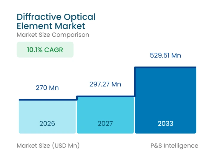
Revenue in the global diffractive optical element market is estimated at USD 270.00 Million for 2026 and is projected to rise to USD 297.27 Million in 2027. Sales are projected to climb to USD 529.51 Million by 2033, advancing at a CAGR of 10.1% over 2027-2033 as laser, sensing, and chip-equipment programs design more of these parts into new products. Laser system builders, chip-equipment makers, and depth-sensing module assemblers account for most purchases, because one micro-structured part can split, flatten, or pattern a beam that would otherwise need several conventional lenses and careful alignment.
Semiconductor tool builders are among the most demanding buyers in the diffractive optical element market, since lithography illuminators, wafer inspection systems, and laser dicing tools use fused-silica homogenizers and beam splitters. SEMI projects that wafer fab equipment sales will rise 23.1% in 2026, an upward revision it ties to AI-related logic and memory investment. That spending reaches element suppliers only through new tool builds and design-ins. Element makers already qualified with lithography and inspection equipment builders are better positioned to win that work, because requalifying an optical part inside a production tool is slow and expensive for the toolmaker.
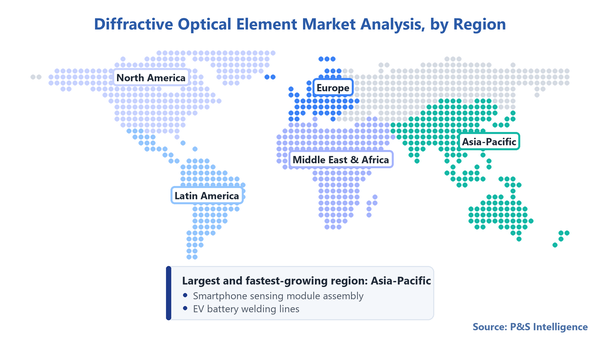
Asia-Pacific held 44.5% of revenue in 2026 and is projected to post the fastest growth, an 11.4% CAGR during 2027-2033. China, Japan, South Korea, and Taiwan host the smartphone sensing-module, EV battery, and chip packaging lines that buy elements in volume, and India is adding new assembly and test plants. North America, the second-largest region, depends more on upgrades to an installed base of industrial lasers, medical lasers, and inspection equipment, so its spending leans toward higher-specification parts than toward new production sites.
Key market insights
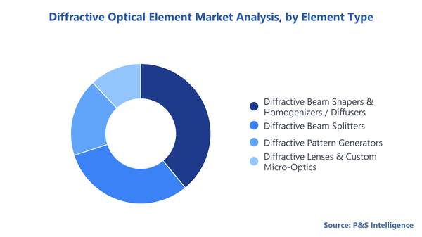
By element type, diffractive beam shapers & homogenizers / diffusers held 39.0% in 2026, while diffractive pattern generators are projected to grow at an 11.6% CAGR during 2027-2033.
By architecture / phase level structure, binary DOEs held 48.0% in 2026, while multi-level DOEs are projected to grow at a 12.3% CAGR during 2027-2033.
By application, laser material processing held 35.0% in 2026 and is also projected to grow at the fastest pace, a 12.5% CAGR during 2027-2033.
By substrate material, fused silica & synthetic quartz held 52.0% in 2026, while optical polymers & resins are projected to grow at a 12.1% CAGR during 2027-2033.
By geography, Asia-Pacific held 44.5% in 2026 and is also projected to grow at the fastest pace, an 11.4% CAGR during 2027-2033.
Diffractive Optical Element Market Growth Drivers & Challenges
Battery and e-motor welding lines are accelerating orders for engineered beam profiles
Laser integrators equipping battery and electric-motor plants are among the most active buyers of diffractive beam shapers. Copper and aluminum busbars reflect most of the incoming laser energy, and a plain Gaussian spot tends to cause spatter and unstable melt pools on cell tabs and hairpin stators. Process engineers therefore fit top-hat, ring, and multi-spot elements into the welding head so energy arrives in a controlled profile. Once a head design is qualified, the same element stays on its bill of materials for every unit built.
According to the IEA, global electric car sales passed 20 million in 2025, about one in four new cars sold worldwide. That figure sizes the vehicle platform base that battery and motor plants serve, not the share of welding lines using diffractive optics, since many lines still run fixed refractive optics or beam oscillation. For element suppliers, the commercial lever is design-in timing. A shaper qualified on a welding head early in a vehicle program tends to ship for the life of that production line.
Wafer-scale lithographic production is transforming supplier cost structures
Element makers are moving production from single-part fabrication to wafer-scale lithography and replication, where many elements are patterned and etched on one substrate. The shift lowers unit cost at volume and makes multi-level phase structures, which need several aligned exposure and etch steps, affordable for more applications. It also raises the fixed cost of staying competitive, because a cleanroom line with steppers and etch tools pays back only when it runs near capacity across several customer programs.
Jenoptik confirms that its Dresden fab, opened on May 6, 2025 after an investment of just under USD 112.17 Million (EUR 100 Million), makes micro-optics exclusively in ISO 5 and ISO 3 cleanrooms, with 2,000 square meters of cleanroom production space, and names the semiconductor equipment industry as its main market. Capacity on that scale favors producers able to spread fab overhead across lithography, laser-processing, and inspection accounts. Smaller design houses without their own lithography lines are more likely to rely on foundry partners for volume, which shifts their margin toward design and application engineering.
Near-eye display waveguides are opening a volume channel for surface relief gratings
Smart-glasses developers need waveguide combiners that carry a projected image through a thin lens into the wearer's eye, and nanoimprinted surface relief gratings are one established way to build them. Each eyepiece needs its own in-coupling and out-coupling gratings, so grating content per device is set by the optical design. If a consumer smart-glasses product reaches volume, demand would shift from prototype quantities to wafer-scale orders for grating masters, imprint stamps, and replicated waveguide parts.
In a January 6, 2025 notice, NIL Technology said that Radiant Opto-Electronics, a Taiwanese backlight-module maker, had completed its acquisition of the Danish nanostructure specialist, which counts meta-optics, diffractive optics, and advanced gratings among its capabilities. A display-module producer buying grating know-how indicates that high-volume panel makers see near-eye optics as an adjacent business. Producers combining imprint capacity with display-module scale could capture grating orders early, while specialist designers would compete on field of view and optical efficiency.
Wavelength-specific custom design is limiting sales to smaller laser users
Each diffractive element is computed for one wavelength, input beam size, and working distance, so a change of laser source or optical layout usually means a new design, a new photomask, and fresh qualification runs. For machine builders and research groups, that turns a component purchase into an engineering project with design fees and longer lead times. University laboratories and small integrators often keep refractive optics that tolerate a wider operating window, which narrows the technology's reach among smaller accounts.
Catalog stocking is starting to ease that barrier. Edmund Optics announced on July 14, 2025 that it now carries Holo/Or diffractive diffusers and beamsplitters off the shelf with transparent pricing, with the beamsplitters optimized for 355 nm, 532 nm, 1064 nm, and 10.6 μm laser lines. Stock parts matched to common industrial wavelengths let small integrators trial a diffractive layout without paying design fees. Applications outside those laser lines still depend on custom engineering, so the restraint eases mainly for mainstream laser processing.
Segmentation Analysis
Element Type
Diffractive Beam Shapers & Homogenizers / Diffusers accounted for 39.0% of diffractive optical element market revenue in 2026. Welding, cutting, and surface-treatment lasers need even energy across the spot, and every new laser head designed for those processes opens a potential shaper slot. Holo/Or cites a trial by Blackbird Robotersysteme in which ring-shaped beam profiles raised welding speed by 40% against the maximum possible with a Gaussian beam. Gains of that size let integrators justify a custom shaper on throughput alone, which ties this category to capital spending on production lasers.
Diffractive Pattern Generators are projected to grow at an 11.6% CAGR during 2027-2033, the fastest pace in this axis. Depth cameras, robot vision systems, and structured-light scanners project dot, line, and grid patterns to measure shape and distance, and each structured-light module carries at least one pattern element. These projectors run infrared lasers near people's eyes, so they are classified under IEC 60825-1, the international laser product safety standard, whose Class 1 covers products safe under reasonably foreseeable operating conditions. Elements that suppress the zero-order hot spot help module makers stay within that class without cutting output power.
Copyright P&S Intelligence. Reuse requires attribution under CC BY 4.0.
Architecture / Phase Level Structure
Binary DOEs held 48.0% of revenue in 2026. A two-level profile needs one mask and one etch step, so binary elements are the cheapest to design, prototype, and reproduce, and they cover high-volume beam splitters, gratings, and pattern projectors where the efficiency of a two-level profile is acceptable. Short development cycles also suit integrators that change laser layouts often. For high-volume buyers, the low tooling cost per design keeps binary parts the default choice whenever efficiency is not the limiting specification.
Multi-Level DOEs are projected to grow at a 12.3% CAGR during 2027-2033, the fastest in this axis. A 1991 Optics Letters study from the Technion gives theoretical diffraction efficiencies of 40.5% for two phase levels, 81.1% for four, 95.0% for eight, and 98.7% for sixteen. That gap matters to operators of multi-kilowatt welding lasers, lithography illuminators, and battery-powered sensors, where light sent into unwanted orders wastes power or creates hot spots. Wafer-scale lithography lines that align several exposures accurately are making four- and eight-level parts cheaper to produce.
Application
Laser material processing accounted for 35.0% of revenue in 2026. Cutting, welding, marking, micro-machining, and additive manufacturing systems use splitters or shapers to raise throughput per laser. Machine builders buy these elements as engineered parts of their scan heads and processing optics, and ownership ties between optics and scanner makers reinforce that link. SCANLAB stated in 2020 that its parent, TechInvest Holding, had taken a 25% stake in Holo/Or, with closer cooperation expected to widen the application fields for its scan systems.
Laser Material Processing is also projected to post the fastest growth, at a 12.5% CAGR during 2027-2033. Battery welding, semiconductor packaging, and printed-circuit micro-via drilling are adding processes in which one ultrafast or fiber laser is split into many parallel spots, so the number of elements per machine rises with each new line. Each new processing recipe usually needs its own element design, which adds design revenue on top of unit sales and keeps integrators returning to the same qualified supplier.
Substrate Material
Fused silica & synthetic quartz held 52.0% of revenue in 2026, because high-power lasers, deep-ultraviolet lithography, and inspection optics need a substrate that transmits short wavelengths and holds its shape under heat. Corning's HPFS ArF-grade specification certifies internal transmittance of at least 99.5% per centimeter at 193 nm. Properties of that kind let one etched element serve lasers from the ultraviolet to the near-infrared, which keeps fused silica the default for semiconductor equipment builders and kilowatt-class laser integrators.
Optical polymers & resins are projected to grow at a 12.1% CAGR during 2027-2033, the fastest among substrates. Injection molding and resin replication turn one master into very large production runs at a low part price, which suits consumer sensing modules, automotive displays, and machine-vision projectors working at low laser power. NALUX states in its kinoform data sheet that high-precision mold processing makes mass production of plastic lenses with diffractive kinoform surfaces possible. As sensing volumes rise, molders with in-house mastering could gain share in low-power uses, while high-power work stays on glass.
The following segments are analyzed in this report.
Asia-Pacific diffractive optical element market outlook
Asia-Pacific accounted for 44.5% of diffractive optical element market revenue in 2026, and its projected 11.4% CAGR over 2027-2033 is the quickest of any region. The region combines the largest concentration of smartphone and sensing-module assembly, EV battery and motor production, and semiconductor packaging, and each of these buys pattern generators, shapers, or splitters through equipment and module builders. China, the region's largest market, pairs high-volume laser machine building with battery and electronics plants that install those machines locally.
India is the region's fastest-growing market, as new chip assembly and fabrication projects create first-time buyers of lithography, inspection, and laser-marking tools. As per the Prime Minister's Office of India, a May 2026 Cabinet approval of two more units in Gujarat, with combined investment of more than USD 410.95 Million (INR 3,900 Crore), took the number of projects approved under the India Semiconductor Mission to 12. Each plant that starts production is likely to add equipment purchases that carry diffractive parts. Japan, South Korea, and Taiwan add upgrade demand from established fabs and sensing-module suppliers.
Asia-Pacific's lead is likely to widen through 2033 because new capacity keeps adding equipment slots, while mature regions grow mostly through upgrades. Element makers based in the region, such as Focuslight in China and AGC and NALUX in Japan, sit close to these module and tool builders, which shortens qualification and favors suppliers with local production. Export controls on advanced chip tools could slow some Chinese fab projects, which would move part of that demand toward packaging and consumer sensing lines.
Copyright P&S Intelligence. Reuse requires attribution under CC BY 4.0.
North America market analysis
North America trails Asia-Pacific in size, with demand concentrated in upgrades to an installed base of industrial lasers, medical laser platforms, defense optics, and semiconductor inspection tools. Equipment makers here tend to specify custom, higher-value elements such as multi-level shapers and fused-silica splitters, so revenue growth depends more on value per part than on unit counts. Edmund Optics, Coherent, and Broadcom anchor regional supply across catalog, laser, and optical-interconnect channels.
Semiconductor Industry Association data show more than 160 announced U.S. semiconductor supply-chain projects across 30 states since 2020, in a tally updated on September 22, 2026. Announced investment is not the same as installed equipment, and many projects span a decade, so the count signals future tool demand and not current orders. As fabs and packaging plants come online, element suppliers already qualified with U.S. inspection and lithography toolmakers are better positioned to win the added design-ins.
Europe market analysis
Europe carries more weight in high-specification optics than its revenue share suggests, with Germany home to lithography optics, laser-source, and micro-optics producers that sell into global equipment programs. Much of Europe's element demand therefore follows export orders for machines built in Germany, Switzerland, and the Netherlands, and less of it comes from local factory construction. That export dependence makes regional growth sensitive to the investment cycles of overseas equipment buyers.
In its June 2025 member survey, the VDMA laser and photonics working group found that only 19% of respondents expected domestic orders to rise that year, against 34% expecting a decline, while 41% expected international orders to grow. Weak home investment slows upgrade spending by European factories, but export programs for lithography, inspection, and laser tools keep design work flowing to European element makers. Producers with strong positions in semiconductor equipment chains are less exposed to the domestic slowdown.
Latin America market analysis
Latin America accounts for a small share of global demand, concentrated in Mexico and Brazil, where automotive, appliance, and electronics plants buy laser marking, cutting, and welding systems from foreign machine builders. Diffractive elements enter the region mostly inside imported equipment, so local purchasing follows plant investment cycles. Machine builders and integrators with service teams in Mexico are the main route through which these parts reach end users.
INEGI recorded light-vehicle production in Mexico of 2,946,943 units in January-September 2026, down 2.4% year on year, with 2,528,623 units exported over the same period. Those figures size the vehicle platform base served by Mexican plants, not the use of diffractive optics on their lines. A softer production year delays new laser-cell purchases, though electrification programs at export-oriented plants could add welding and marking stations once model changeovers resume.
Middle East & Africa market analysis
The Middle East & Africa contributes the smallest share, with demand split between a design-led cluster in Israel and early-stage industrial and research buying in the Gulf states and South Africa. Israeli laser, medical-device, and defense-electronics developers specify custom splitters and shapers for systems that are largely exported, and Holo/Or designs and produces elements in Ness Ziona. These developers buy in small lots but at a high value per part, since each element is engineered for one specific system.
The Israel Innovation Authority puts high-tech exports at 58% of Israel's total exports in 2025, a record share. That export base supports steady design work for local element suppliers, whose order books follow foreign system sales more than domestic factory building. In the Gulf, new manufacturing and research programs are more likely to buy finished laser and sensing systems than to specify custom elements, which keeps regional purchases small through the forecast period.
The following geographies are analysed in this report.
Asia-Pacific
China
Japan
South Korea
Taiwan
India
Australia
Rest of Asia-Pacific
Europe
Germany
U.K.
France
Italy
Netherlands
Spain
Rest of Europe
Latin America
Brazil
Mexico
Rest of Latin America
Middle East & Africa
Saudi Arabia
U.A.E.
South Africa
Rest of Middle East & Africa
North America
U.S.
Canada
Diffractive Optical Element Market Competition Analysis
The diffractive optical element market is moderately fragmented, with supply spread across optics groups, wafer-level producers, and design specialists, and no single company covers every application, wavelength, and volume tier. Elements are designed to order for each laser, sensor, or tool, so qualification with a specific equipment program, access to lithography and etch capacity, and application engineering skill count for more than catalog breadth. Switching costs are high once an element is designed into a production tool or sensing module, because requalification means new test runs for the buyer.
Large optics and materials groups such as Carl Zeiss AG, Jenoptik AG, Coherent Corp., and AGC Inc. compete on fab capacity, substrate know-how, and long qualification histories with lithography, laser, and sensing customers. Wafer-level and molding specialists including Focuslight Technologies Inc., NALUX Co., Ltd., and Nissei Technology Corporation compete on unit cost for high-volume consumer and automotive programs. Design-focused specialists such as Holo/Or Ltd., HOLOEYE Photonics AG, and SILIOS Technologies SAS win work through custom engineering for high-power lasers, research instruments, and short-run industrial jobs.
The structure is shifting slowly as acquisitions fold specialist designers and wafer-level producers into larger optics and display groups, which brings design skill and volume capacity under one roof. Focuslight's 2024 purchase of SUSS MicroOptics, now Focuslight Switzerland SA, is one example. For buyers, sourcing tends to follow power class and volume. High-power and semiconductor programs gravitate toward suppliers with fused-silica fabs and long qualification records, while consumer and automotive sensing programs favor molders and wafer-level producers that can quote low unit prices at scale.
Major Companies in Diffractive Optical Element Market:
Carl Zeiss AG
Coherent Corp.
Jenoptik AG
Holo/Or Ltd.
Broadcom Inc.
AGC Inc.
HOLOEYE Photonics AG
NALUX Co., Ltd.
Edmund Optics Inc.
Focuslight Technologies Inc.
Nissei Technology Corporation
LightTrans International GmbH
SILIOS Technologies SAS
Diffractive Optical Element Market News
In August 2026, Jenoptik AG reported that first-half order intake in its Semiconductor & Advanced Manufacturing unit rose 85.3%, driven by lithography and inspection demand, lifting the group book-to-bill ratio to 1.44. The order surge signals heavier spending on precision optical subsystems by chip-equipment makers, a core buyer group for micro-optics.
In July 2026, Carl Zeiss AG disclosed that its semiconductor manufacturing technology unit is adding about 25,000 square meters of production and production-related space in Oberkochen, Germany, with a multifunctional factory under construction in Wetzlar, to serve High-NA EUV optics, photomask, and wafer inspection work. The build-out enlarges the optical supply base behind lithography and inspection tools, one of the main end uses for fused-silica beam-shaping elements.
In January 2026, AGC Inc. exhibited glass diffractive optical elements and glass diffusers for high-accuracy 3D sensing at CES 2026 in Las Vegas (booth 6653, January 6-9), with design-to-evaluation support for module makers. Glass elements with low zero-order transmission give sensing-module makers a more durable alternative to polymer parts.
Last Updated: October 2026
Frequently Asked Questions About This Report
How big is the diffractive optical element market?+
Revenue in the global diffractive optical element market is estimated at USD 270.00 Million for 2026 and is projected to rise to USD 297.27 Million in 2027.
What is the growth rate of the diffractive optical element market?+
Sales are projected to climb to USD 529.51 Million by 2033, advancing at a CAGR of 10.1% over 2027-2033 as laser, sensing, and chip-equipment programs design more of these parts into new products.
Who buys diffractive optical elements and why?+
Laser system builders, chip-equipment makers, and depth-sensing module assemblers account for most purchases, because one micro-structured part can split, flatten, or pattern a beam that would otherwise need several conventional lenses and careful alignment.
Which region dominates the diffractive optical element market?+
Asia-Pacific accounted for 44.5% of diffractive optical element market revenue in 2026, and its projected 11.4% CAGR over 2027-2033 is the quickest of any region.
What are diffractive optical elements used for in industry?+
Laser material processing accounted for 35.0% of revenue in 2026. Cutting, welding, marking, micro-machining, and additive manufacturing systems use splitters or shapers to raise throughput per laser.
What material are diffractive optical elements made of?+
Fused silica & synthetic quartz held 52.0% of revenue in 2026, because high-power lasers, deep-ultraviolet lithography, and inspection optics need a substrate that transmits short wavelengths and holds its shape under heat.
Who are the top diffractive optical element manufacturers?+
Large optics and materials groups such as Carl Zeiss AG, Jenoptik AG, Coherent Corp., and AGC Inc. compete on fab capacity, substrate know-how, and long qualification histories with lithography, laser, and sensing customers.
Want a report tailored exactly to your business need?
Leading companies across industries trust us to deliver data-driven insights and innovative solutions for their most critical decisions. From data-driven strategies to actionable insights, we empower the decision-makers who shape industries and define the future. From Fortune 500 companies to innovative startups, we are proud to partner with organisations that drive progress in their industries.
Client Testimonials
Working with P&S Intelligence and their team was an absolute pleasure – their awareness of timelines and commitment to value greatly contributed to our project's success. Eagerly anticipating future collaborations.
McKinsey & Company
India
Unmatched Standards
Our insights into the minutest levels of the markets, including the latest trends and competitive landscape, give you all the answers you need to take your business to new heights
Complete Data Security
We take a cautious approach to protecting your personal and confidential information. Trust is the strongest bond that connects us and our clients, and trust we build by complying with all international and domestic data protection and privacy laws