This Report Provides In-Depth Analysis of the Chiplet Packaging Market Report Prepared by P&S Intelligence, Segmented by Packaging Technology (2.5D packaging, 3D packaging, Fan-out multi-die packaging, Advanced system-in-package, Other chiplet-enabled packaging), Application (Data center, high-performance computing, and AI, Consumer electronics, Communications and networking, Automotive, Industrial, aerospace, and defense, Other applications), Buyer / Service Model (Merchant foundry and OSAT packaging services, Captive IDM and foundry packaging, Outsourced packaging engineering and test, Integrated turnkey packaging), and Geographical Outlook for the Period of 2021 to 2032
Explore the market potential with our data-driven report
Chiplet Packaging Market Overview
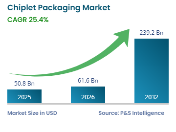
The global chiplet packaging market size is estimated at USD 50.8 billion in 2025 and is projected to reach USD 61.6 billion in 2026 and USD 239.2 billion by 2032, advancing at a 25.4% CAGR from 2026 to 2032. Demand centers on packages that combine separately manufactured compute, memory, and input/output dies when a monolithic design would face yield, bandwidth, or reticle constraints.
Commercial value is moving toward package-level co-design, high-density interconnects, and known-good-die testing. TSMC reported that its 3-nanometer system-on-integrated-chip stacking technology entered volume production in 2025. Amkor Technology Inc. also reported record advanced-packaging revenue for 2025, indicating that external assembly and test providers are participating in the expansion.
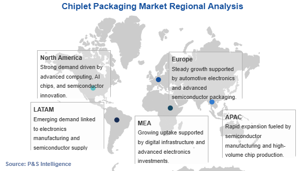
Asia-Pacific holds the largest chiplet packaging market share at 46% in 2025. The region combines foundries, outsourced semiconductor assembly and test providers, memory producers, substrate suppliers, and electronics manufacturing capacity. North America accounts for 31%, supported by processor designers, hyperscale computing demand, and investment in domestic advanced-packaging production. Asia-Pacific is also expected to expand fastest at a 16.0% CAGR through 2032.
The outlook remains sensitive to qualification schedules, substrate availability, thermal management, and the pace at which announced capacity reaches production. The model excludes chiplet silicon and finished-processor revenue, keeping the forecast focused on packaging and related assembly and test value.
Key Market Insights
By packaging technology, 2.5D packaging leads with a 55% share in 2025, while 3D packaging is projected to grow fastest at a 19.0% CAGR from 2026 to 2032.
By application, data center, high-performance computing, and AI lead with a 62% share in 2025 and are projected to grow fastest at an 18.0% CAGR from 2026 to 2032.
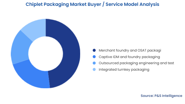
By buyer / service model, merchant foundry and OSAT packaging services lead with a 48% share in 2025, while integrated turnkey packaging is projected to grow fastest at a 17.5% CAGR from 2026 to 2032.
By geography, Asia-Pacific leads with a 46% share in 2025 and is projected to grow fastest at a 16.0% CAGR from 2026 to 2032.
Chiplet Packaging Market Trends and Growth Drivers
AI systems are increasing the value of high-density multi-die integration
Demand for AI accelerators and high-performance processors is making the package a central system-design decision. Compute dies need short, dense links to high-bandwidth memory and input/output functions, while separately manufactured dies must be screened before final assembly. Intel Foundry reports that it has produced more than 100 2.5D designs at scale and offers advanced chiplet testing to identify known-good dies. That installed experience supports the move from single-die packages toward larger heterogeneous assemblies.
This shift supports chiplet packaging market growth because each package can require interposers or bridges, fine-pitch bonding, redistribution, thermal engineering, and more extensive test flows. The effect is strongest where bandwidth and power efficiency justify the additional integration cost. It is weaker in cost-sensitive devices that can meet requirements with conventional packaging.
Local capacity and turnkey services can broaden access beyond captive supply chains
The chiplet packaging industry has an opportunity to serve designers that do not control a complete foundry, interposer, assembly, and test chain. Integrated providers can coordinate design rules, wafer sort, known-good-die selection, substrate or interposer sourcing, assembly, and final test. A coordinated flow can reduce handoff risk and give fabless companies a clearer route to qualification, although it does not eliminate yield or thermal challenges.
Capacity localization reinforces this opening. The U.S. Department of Commerce outlined up to USD 1.6 billion for advanced-packaging research areas that included chiplet ecosystems, thermal management, connectors, and co-design. Amkor Technology Inc. later expanded its planned Arizona packaging campus to about 93,000 square meters of cleanroom space across two phases. These programs can widen qualified supply if construction, equipment installation, and customer ramps remain on schedule.
Standardized interfaces and hybrid bonding are reshaping package roadmaps
Interoperability and denser vertical connections are important chiplet packaging industry trends. The UCIe Consortium released its 3.0 specification with data rates of 64 GT/s, while its earlier 2.0 specification added support for 3D packaging and hybrid-bond pitches extending to 1 micrometer or less. A common interface framework can make it easier to combine dies from different design teams or process technologies without defining every connection from scratch.
Packaging roadmaps are therefore moving beyond conventional micro-bumps toward finer direct connections, while still retaining 2.5D interposers, bridges, and fan-out structures where they offer better cost, yield, or thermal tradeoffs. Standardization supports ecosystem development, but it does not guarantee that independently sourced chiplets will meet shared power, thermal, test, and reliability requirements.
Thermal, test, and yield risks limit deployment in cost-sensitive devices
Adding dies increases the number of interfaces that must function after assembly. A defect in one component or bond can reduce the value recovered from the other known-good dies, and tighter spacing can concentrate heat within the package. These risks raise the importance of wafer sort, die traceability, package-level simulation, system-level testing, and application-specific reliability qualification.
The commercial restraint is strongest when expected performance gains do not cover the higher engineering, substrate, assembly, cooling, and validation costs. Capacity expansion alone will not remove this barrier because process maturity and customer qualification develop over multiple production cycles.
Chiplet Packaging Market Segmentation Analysis
Packaging Technology
2.5D packaging holds the largest share, accounting for 55% in 2025. The chiplet packaging market analysis attributes this position to mature interposer and bridge architectures that place logic and high-bandwidth memory side by side. Intel Foundry has produced more than 100 2.5D designs at scale, providing a separate indicator of production maturity rather than merely restating the modeled share. Silicon interposers offer high routing density, while embedded bridges and organic approaches can reduce interposer area or cost for selected designs.
3D packaging is projected to grow fastest at a 19.0% CAGR from 2026 to 2032. Its growth is supported by shorter vertical interconnect paths and higher bandwidth density. UCIe support for 3D packaging and hybrid-bond pitches down to 1 micrometer or less gives designers a more standardized path for fine-pitch stacks. Adoption will remain selective where thermal removal, wafer compatibility, repairability, or stacked-die yield makes a 2.5D design more economical.
Application
Data center, high-performance computing, and AI account for the largest application share at 62% in 2025. These systems combine accelerators, CPUs, custom ASICs, high-bandwidth memory, and input/output dies in packages that must sustain high data rates. SK hynix Inc. broke ground on an Indiana advanced-packaging facility backed by an investment of more than USD 4 billion for next-generation high-bandwidth memory, a distinct capacity commitment aligned with AI package demand.
The same application is projected to grow fastest at an 18.0% CAGR from 2026 to 2032. Continued scaling of model training, inference, cloud services, and high-performance computing increases the need for memory bandwidth and package-level compute density. The growth rate remains conditional on data-center capital spending, accelerator demand, power availability, and the ability of packaging suppliers to qualify larger assemblies without unacceptable thermal or yield penalties.
Buyer / Service Model
Merchant foundry and OSAT packaging services lead with a 48% share in 2025. Their position reflects the cost of specialized bonding, redistribution, metrology, assembly, and test equipment that can be shared across customer programs. Advanced Semiconductor Engineering Inc. held a groundbreaking ceremony in October 2025 for its NT$17.6 billion K18B factory, which is planned for CoWoS-related processes, system-in-package applications, and chiplet-capable technologies. The project provides a separate measure of external capacity investment.
Integrated turnkey packaging is projected to grow fastest at a 17.5% CAGR from 2026 to 2032. Buyers can use a coordinated flow that connects wafer sort, package design, interposer or substrate management, assembly, and final test. The driver is reduced coordination burden across suppliers, particularly for fabless designers entering multi-die products. Growth depends on providers proving yield accountability and data continuity across process steps rather than merely bundling services contractually.
The complete segmentation hierarchy is as follows:
Packaging Technology
2.5D packaging
3D packaging
Fan-out multi-die packaging
Advanced system-in-package
Other chiplet-enabled packaging
Application
Data center, high-performance computing, and AI
Consumer electronics
Communications and networking
Automotive
Industrial, aerospace, and defense
Other applications
Buyer / Service Model
Merchant foundry and OSAT packaging services
Captive IDM and foundry packaging
Outsourced packaging engineering and test
Integrated turnkey packaging
Drive strategic growth with comprehensive market analysis
Chiplet Packaging Market Geographical Analysis
Asia-Pacific is the largest region, with 46% of revenue in 2025, and its 16.0% CAGR through 2032 makes it the fastest regional contributor to chiplet packaging market growth. The region combines leading foundries, OSATs, memory producers, substrate suppliers, and equipment ecosystems. TSMC reported that its 3-nanometer system-on-integrated-chip stacking technology entered volume production in 2025, while Advanced Semiconductor Engineering Inc. held a groundbreaking ceremony for a planned NT$17.6 billion factory in Kaohsiung for advanced packaging and system-in-package applications. This production milestone and planned capacity expansion are consistent with the region's approved leading position as AI and high-performance computing packages move into higher volumes. The trajectory would weaken if qualified capacity shifted faster than expected to North America.
North America accounts for 31% of the market in 2025 and is projected to advance at a 14.5% CAGR through 2032. Its mechanism differs from Asia-Pacific because demand ownership and package design are stronger than current high-volume manufacturing depth. In September 2026, Amkor Technology Inc. expanded its planned U.S. outsourced advanced-packaging campus to about 93,000 square meters of cleanroom capacity across two phases and raised expected investment to approximately USD 12 billion. The region should gain additional production capability as the campus reaches production qualification, but delayed construction, limited substrate availability, or slower customer ramps would preserve dependence on Asian supply.
Taiwan is the leading country in Asia-Pacific in 2025. Its position rests on the proximity of TSMC's CoWoS and SoIC platforms, ASE's VIPack capabilities, substrate partners, and a deep semiconductor manufacturing workforce. TSMC describes CoWoS as experiencing strong growth from AI demand, and its 2025 report confirms continued investment in advanced packaging facilities in Taiwan. This base supports a trajectory of larger interposer formats, denser stacking, and additional OSAT participation through 2032. Taiwan's share could soften if overseas facilities duplicate leading processes at scale or if local capacity expansion and customer qualification take longer than planned.
The U.S. represents 90% of North America revenue in 2025. Its position reflects headquarters demand from processor, accelerator, networking, cloud, and system companies as well as expanding domestic packaging capacity. Amkor broke ground on its Arizona advanced-packaging campus in October 2025, and SK hynix Inc. followed with an Indiana groundbreaking in August 2026 for a next-generation high-bandwidth-memory packaging facility supported by more than USD 4 billion of investment. These projects can connect U.S. design demand with local assembly and test. The trajectory depends on production qualification beginning as scheduled, and it would shift downward if equipment, workforce, or customer-ramp delays postpone commercial output.
Geographies covered in this report are;
North America
U.S.
Canada
Europe
Germany
U.K.
France
Netherlands
Italy
Spain
Rest of Europe
Asia-Pacific
Taiwan
South Korea
China
Japan
Singapore
India
Rest of Asia-Pacific
Latin America
Brazil
Mexico
Rest of Latin America
Middle East & Africa
U.A.E.
Saudi Arabia
South Africa
Rest of Middle East & Africa
Chiplet Packaging Market Competitive Landscape
The chiplet packaging market has moderately consolidated competitive structure. Process ownership gives foundries and IDMs control over differentiated integration platforms, while OSATs compete through customer flexibility, package breadth, test capability, and geographic reach. The chiplet packaging industry is therefore neither fully captive nor an interchangeable merchant-service market. Buyers often qualify a package around a provider's design rules, interconnect process, materials, and test flow, which raises switching costs after production begins.
Foundry-led competition centers on co-optimization. Taiwan Semiconductor Manufacturing Company Limited combines CoWoS horizontal integration with SoIC stacking. Intel Corporation competes through EMIB bridges, Foveros stacking, and advanced chiplet test. Samsung Electronics Co. Ltd. links its I-Cube and X-Cube platforms with internal foundry and memory capabilities. These models can shorten coordination across wafer and package processes, but they may also increase buyer dependence on one qualified ecosystem.
OSAT competition emphasizes external access and execution. ASE Technology Holding Co. Ltd., through Advanced Semiconductor Engineering Inc., offers fan-out, 2.5D, 3D, and co-packaged-optics capabilities under VIPack. Amkor Technology Inc. competes through packaging and test services alongside an expanding production footprint. Their opportunity is to provide second-source options and turnkey coordination for customers that want alternatives to captive flows.
Entry barriers include fine-pitch process control, thermal and mechanical modeling, known-good-die data, substrate access, reliability qualification, and the capital needed for bonding, redistribution, metrology, and test. Competition should intensify as new capacity enters service, although customer qualification cycles and production learning are likely to prevent rapid commoditization.
Key Players in the Chiplet Packaging Market:
Taiwan Semiconductor Manufacturing Company Limited
In August 2026, SK hynix Inc. held a groundbreaking ceremony for an advanced HBM packaging facility in West Lafayette, Indiana, backed by more than USD 4 billion of investment. The company targets mass production in the second half of 2029, adding a future U.S. supply option for AI memory.
In October 2025, Amkor Technology Inc. broke ground on an advanced packaging and test campus in Peoria, Arizona, planned in two phases. The first facility is scheduled for completion in mid-2027, with production expected to begin in early 2028.
In October 2025, Advanced Semiconductor Engineering Inc. broke ground on its K18B factory in Kaohsiung, Taiwan. The NT$17.6 billion project is scheduled for completion in the first quarter of 2028 and will support CoWoS-related processes, system-in-package production, and chiplet-capable packaging technologies.
Want a report tailored exactly to your business need?
Leading companies across industries trust us to deliver data-driven insights and innovative solutions for their most critical decisions. From data-driven strategies to actionable insights, we empower the decision-makers who shape industries and define the future. From Fortune 500 companies to innovative startups, we are proud to partner with organisations that drive progress in their industries.
Client Testimonials
Working with P&S Intelligence and their team was an absolute pleasure – their awareness of timelines and commitment to value greatly contributed to our project's success. Eagerly anticipating future collaborations.
McKinsey & Company
India
Unmatched Standards
Our insights into the minutest levels of the markets, including the latest trends and competitive landscape, give you all the answers you need to take your business to new heights
Complete Data Security
We take a cautious approach to protecting your personal and confidential information. Trust is the strongest bond that connects us and our clients, and trust we build by complying with all international and domestic data protection and privacy laws