This Report Provides In-Depth Analysis of the Chiplet Interposer Inspection and Repair Equipment Market Report Prepared by P&S Intelligence, Segmented by Equipment Type (Inspection Systems, Metrology Systems, Repair and Rework Systems), Inspection Technology (Optical Inspection, X-ray Inspection, Acoustic Inspection, Infrared Inspection), Integration Type (2.5D Interposer-Based Integration, 3D Stacked Integration), End User (OSATs, Foundries, Integrated Device Manufacturers (IDMs), Research Institutes), Deployment (Inline Inspection, Offline and Sampling Inspection, Failure Analysis and Process Development), and Geographical Outlook for the Period of 2022 to 2033
Chiplet Interposer Inspection and Repair Equipment Market Statistics
Key Highlights
Study Period
2022 - 2033
Market Size in 2026
USD 1.53 Billion
Market Size in 2027
USD 1.71 Billion
Market Size by 2033
USD 3.29 Billion
Projected CAGR
11.5%
Largest Region
Asia-Pacific
Fastest Growing Region
Asia-Pacific
Market Structure
Moderately Concentrated
Market Size
Explore the market potential with our data-driven report
Chiplet Interposer Inspection and Repair Equipment Market Overview
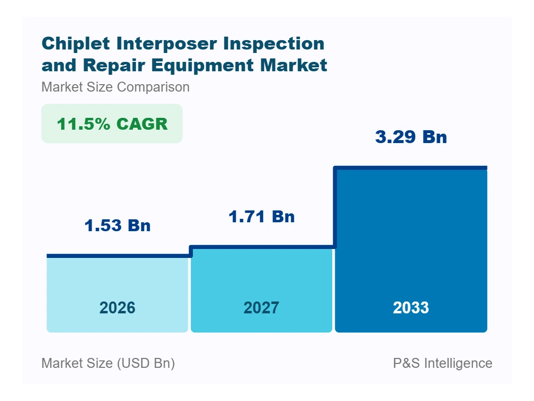
The global chiplet interposer inspection and repair equipment market size is estimated at USD 1.53 Billion in 2026 and is projected to reach USD 1.71 Billion in 2027. The market is expected to climb to USD 3.29 Billion by 2033, a CAGR of 11.5% during 2027-2033, as AI accelerator and HBM output expands. Foundries, OSATs, and memory makers are adding inspection points to these lines because a single faulty interposer, bump, or bonded die can scrap a module that already carries several costly logic and memory chips.
Hybrid bonding and taller memory stacks are multiplying the checkpoints on chiplet packaging lines, and the foundries and assembly houses running those lines tend to add inspection capacity with each new bonder. According to SEMI, assembly and packaging equipment sales are projected to rise 9.6% to USD 6.7 Billion in 2026, a category that does not isolate inspection spending. That bonding capacity sets the pace for inspection orders, since every bonding stage needs optical, X-ray, or acoustic screening before more dies are committed to the package. For equipment vendors, revenue follows packaging capacity additions more closely than front-end fab cycles.
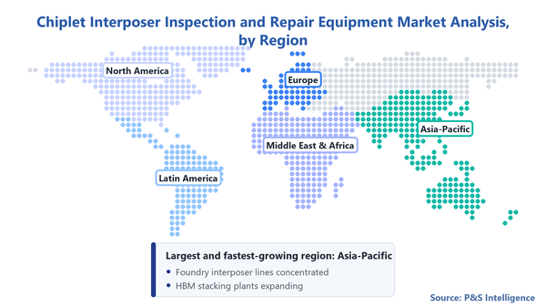
Asia-Pacific accounts for 70% of the chiplet interposer inspection and repair equipment market in 2026 and is projected to grow fastest, at a 12.8% CAGR during 2027-2033. Taiwan's foundry-run CoWoS and SoIC lines, South Korea's HBM stacking plants, and OSAT sites in China, Malaysia, and Singapore keep most tool shipments in the region. North America and Europe buy on a different basis, equipping smaller domestic packaging and pilot lines whose order volumes depend on public funding and the pace of new site construction.
Key market insights
By equipment type, inspection systems account for the largest share in 2026.
By inspection technology, optical inspection accounts for 37% in 2026.
By integration type, 3D stacked integration leads in 2026 and is set to expand at a 12.1% CAGR over 2027-2033.
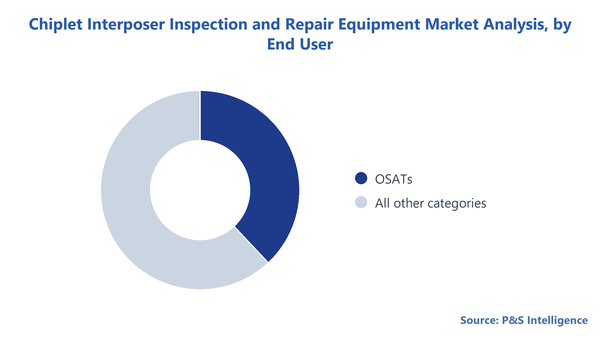
By end user, OSATs account for 38% in 2026 and are forecast to post an 11.7% CAGR during 2027-2033.
By deployment, inline inspection accounts for 47% in 2026.
By geography, Asia-Pacific accounts for 70% in 2026 and is expected to advance at a 12.8% CAGR over 2027-2033.
Taller memory stacks are reshaping inspection toward per-layer screening
High-bandwidth memory makers are moving toward taller DRAM stacks, and every added layer brings another bonding interface that can hide voids, misaligned micro-bumps, or die cracks. Electrical test reaches many of these buried faults only after the full stack is assembled, so memory manufacturers screen interfaces optically or acoustically as layers go on. Inspection spending shifts from end-of-line checks toward repeated in-flow passes on every stacking line, which raises the tool count needed per unit of HBM output.
JEDEC's HBM4 standard, released in April 2025, defines stack configurations from 4-high to 16-high, with a 16-high cube reaching 64 GB at 32 Gb die density. A 16-high cube carries four more bonded interfaces than a 12-high one, which adds inspection passes per finished part on the same wafer output. Tool suppliers that resolve sub-micron voids at stacking-line throughput are better positioned when memory makers select the tool of record for each new generation.
Finer bonding interconnects are driving more inspection steps per package
Foundries and OSATs building 2.5D and 3D packages for AI accelerators are tightening bump pitches and moving toward copper-to-copper hybrid bonds, which leave less margin for particles, voids, and overlay error. A defect missed before bonding is sealed inside the package, and every die already attached is lost with it. Process engineers respond by adding inspection or metrology after each critical bonding step.
KLA Corporation's fiscal 2026 Form 10-K credits growth in its advanced packaging business to the rising complexity and value of semiconductor packages, particularly for AI and high-performance computing. Higher package value raises the cost of each escaped defect, which justifies more inspection steps per wafer at the same packaging output. Equipment demand can therefore grow faster than package volumes, and platforms that cover several inspection and metrology steps on one tool tend to appeal to packaging lines short on floor space.
Subsidized packaging plants are creating first-time tool orders
Governments funding domestic assembly and test plants are adding a pool of buyers with no installed inspection base to replace. A greenfield packaging line has to equip every inspection and metrology step at once, and early tool choices often become the reference for later expansions on the same site. For equipment vendors, these sites offer full-line orders, a different sale from the incremental add-on tools that dominate established hubs in Taiwan and South Korea.
Per the India Semiconductor Mission, India's Semicon 2.0 scheme, whose pillars were notified on August 31, 2026, gives advanced packaging projects, a category that covers 2.5D and 3D packaging and heterogeneous integration, fiscal support of 35% of eligible capital expenditure against 25% for legacy packaging. The higher rate lowers the cost of equipping interposer-capable lines, inspection steps included, relative to conventional assembly. Near-term order value from such sites is modest, since new plants usually qualify simpler packages first, but vendors that equip the first lines are better positioned for later 2.5D and 3D upgrades.
Export controls on advanced memory are limiting tool sales into China
Equipment vendors selling into China face a narrower set of buyers for HBM and advanced-logic packaging lines, because US rules restrict both advanced memory and many of the tools used to make chips. Chinese memory makers and OSATs that cannot obtain licensed equipment may delay HBM capacity or turn to domestic tool suppliers, and either path removes orders from foreign inspection vendors. Suppliers with a large share of revenue from mainland China carry the most exposure.
The Bureau of Industry and Security's December 2, 2024 package added controls on high-bandwidth memory and on 24 types of semiconductor manufacturing equipment, and placed 140 entities on the Entity List. The rules are written around device performance and listed tool categories, so their reach into packaging inspection depends on how each system is classified. Even where a tool remains licensable, license reviews lengthen sales cycles and lead vendors to plan shipments around Taiwan, South Korea, and Southeast Asia, which continue to absorb most HBM and CoWoS-class expansion.
Segmentation Analysis
Equipment Type
Inspection systems take the largest share of chiplet interposer inspection and repair equipment market revenue by equipment type in 2026, because they sit at more points in the chiplet flow than any other tool class. Optical, X-ray, and acoustic inspectors screen interposer wafers after via and redistribution-layer formation, check micro-bumps before die attach, and find voids after bonding. The cost of scrapping a bonded AI module keeps engineers from removing inspection points even when they slow the line. Inspectors shared with flip-chip or fan-out lines are counted only for the share of their use on 2.5D and 3D chiplet packages.
Metrology systems serve a narrower role, measuring bump height, coplanarity, and redistribution-layer dimensions where tolerances decide bond yield. Repair and rework systems remove shorts and excess copper on IC substrates before dies are attached, using laser-based automated optical shaping tools such as the Orbotech Ultra PerFix line, and they are counted here only when used on chiplet assemblies. Once chiplets are bonded through micro-bumps or hybrid bonds, rework is rarely practical, so repair spending stays concentrated upstream on the interposer and substrate.
Inspection Technology
Optical inspection holds 37% of inspection-technology revenue in 2026. Optical tools lead because they run fast enough to screen every interposer or HBM wafer inline, they catch the surface and bump defects behind much of the yield loss at these steps, and packaging lines already run optical platforms, which shortens qualification. Current brightfield and darkfield systems also add 3D bump measurement on the same tool, so a single purchase covers defect capture and dimensional checks.
X-ray, acoustic, and infrared tools cover defects that optical systems cannot see. Comet Holding's Yxlon unit introduced the CA20, a fully automated 3D X-ray system for advanced packaging, in November 2023 and says its images identify missing bumps, bridged bumps, and voids in 3D IC connections. Scanning acoustic microscopes from vendors such as Nordson and the Hitachi group find delamination at bond interfaces, while infrared systems such as EV Group's EVG20 image voids through bonded wafer stacks. Buyers add these tools where a buried defect would otherwise surface only at final electrical test.
Integration Type
3D stacked integration leads integration-type revenue in 2026, with high-bandwidth memory as its main volume source. Each HBM cube stacks several DRAM dies on a base die, and memory makers screen every interface before the next die is placed, so inspection passes scale with layer count. Production is concentrated in a small number of memory plants, which means tool orders arrive in large, repeat batches tied to each memory generation's ramp.
3D stacked integration is also set to post the quickest growth, at a 12.1% CAGR during 2027-2033. Hybrid-bonded logic stacks are starting to join HBM in this category, and copper-to-copper bonds without solder tolerate far smaller particles and overlay errors than micro-bumps. Research institute imec recorded die-to-wafer overlay error below 350 nm when hybrid bonding at a 2 µm copper pad pitch, a process that also required copper pad recess under 2.5 nm. For tool vendors, the shift rewards systems that detect sub-micron voids and bonding overlay drift at production speed.
End User
OSATs hold 38% of end-user revenue in 2026. Outsourced assembly houses run chip-on-substrate assembly, final module work, and memory-adjacent packaging for many chip designers at once, so their inspection fleets grow with the number of package programs on their floors. Each new customer program brings its own qualification and recipe set, which tends to add tools as well as reuse existing ones. Large OSATs can also buy in multi-system batches when a foundry partner shifts CoWoS-class volume to them.
OSATs are also projected to grow fastest among end users, at an 11.7% CAGR during 2027-2033. Foundries keep the most advanced bonding steps in-house, but capacity limits can push more of the back half of interposer packaging to outsourced lines, and new OSAT plants in the United States, India, and Southeast Asia must equip inspection from scratch. OSATs qualify tools program by program, which favors vendors with local application engineers who can turn new inspection recipes around quickly.
Copyright P&S Intelligence. Reuse requires attribution under CC BY 4.0.
Deployment
Inline inspection holds 47% of deployment revenue in 2026. High-volume interposer and HBM lines cannot hold a lot for an offline lab result before releasing it to the next bonding step, so they place inspection tools directly in the process flow. Inline tools also return defect data to bonders and plating tools within the same shift, which limits how many wafers a drifting process can damage before engineers intervene.
Offline sampling and failure analysis draw on different budgets. Process development groups and failure-analysis labs at foundries, memory makers, and research institutes buy high-resolution X-ray CT, acoustic, and cross-section tools to find out why a bond failed, then feed the fix back into inline recipes. Unit volumes are lower, but purchases tend to rise with each new package architecture, since a new stack height or bond pitch begins with a characterization phase before volume production starts.
The following segments are analysed in this report.
Equipment Type
Inspection Systems
Metrology Systems
Repair and Rework Systems
Inspection Technology
Optical Inspection
X-ray Inspection
Acoustic Inspection
Infrared Inspection
Integration Type
2.5D Interposer-Based Integration
3D Stacked Integration
End User
OSATs
Foundries
Integrated Device Manufacturers (IDMs)
Research Institutes
Deployment
Inline Inspection
Offline and Sampling Inspection
Failure Analysis and Process Development
Regional Analysis
Asia-Pacific chiplet interposer inspection and repair equipment market outlook
Asia-Pacific accounts for 70% of global revenue in 2026 and is also on track for the quickest expansion, a 12.8% CAGR during 2027-2033. The region hosts the foundry-run interposer and hybrid-bonding lines that produce most AI accelerators, the HBM stacking plants of South Korea's memory makers, and large OSAT clusters in China, Malaysia, and Singapore. Inspection tools follow that capacity, and suppliers sell into the region through local application and service teams that support recipe changes on the production floor.
Taiwan is the region's largest market, built around CoWoS and SoIC capacity that draws inspection orders from foundries and the OSATs sharing their packaging work. Taiwan is also its fastest-growing country, as each added CoWoS-class line brings a new round of tool qualifications. South Korea adds a memory-led channel. SK hynix broke ground in April 2026 on P&T7, a Cheongju fab dedicated to advanced packaging for AI memory such as HBM, which it expects to draw USD 14.25 Billion (KRW 19 Trillion) of investment, and targets its wafer test line for October 2027.
Asia-Pacific's position looks set to strengthen through 2033, because new HBM generations and larger interposers launch first on its lines and each launch resets the inspection tool set. China adds volume through domestic memory and OSAT investment, although export licensing limits which foreign tools can ship there. Singapore and Malaysia add OSAT and memory back-end capacity outside Taiwan, while Japan contributes through packaging research programs and its equipment supply base. For suppliers, many tool-of-record decisions are made in Taiwan and South Korea, so a qualification win at one site often carries over to later capacity at the same customer.
Copyright P&S Intelligence. Reuse requires attribution under CC BY 4.0.
North America market analysis
North America contributes a smaller share, with demand coming from domestic packaging plants under construction, research lines, and the process development groups of US chip designers and IDMs. Purchases here are mostly first-time line fills and pilot tools, which ties order timing to construction milestones and the release of public funding. Buyers also weigh supply security and on-shore service support heavily, because domestic lines must run without the deep local supplier base found in Taiwan or South Korea.
Figures from the U.S. Department of Commerce put its finalized CHIPS award to Amkor Technology Arizona at up to USD 407 Million in direct funding for a greenfield advanced packaging and test facility in Peoria, Arizona. Payments are tied to project milestones, so inspection orders from sites of this kind arrive in phases as each line is commissioned. Suppliers with US-based service teams and experience handling export-control requirements are better positioned for these early lines.
Europe market analysis
Europe holds a smaller, research-weighted share, with purchases led by research institutes, pilot lines, and IDMs building chiplet-based automotive, industrial, and defense products. These buyers favor flexible offline and failure-analysis tools over high-throughput inline fleets, because their volumes are low and their process recipes change often. The region also hosts several inspection suppliers, which gives local buyers short paths to application support and joint development work.
As per Fraunhofer, the APECS pilot line for chiplet and heterogeneous integration technologies, coordinated by the Fraunhofer-Gesellschaft under the EU Chips Act, launched in December 2024 with funding of USD 815.50 Million (EUR 730 Million). Pilot lines of this kind buy small quantities of high-specification X-ray, acoustic, and metrology tools, and their process choices can shape what European IDMs later specify for production. Tool vendors that support these programs gain early sight of the requirements for future regional capacity.
Latin America market analysis
Latin America accounts for a minor share, and commercial demand for chiplet interposer tools is minimal because the region has no volume 2.5D or 3D packaging lines. Existing semiconductor back-end activity in Brazil and Mexico centers on conventional packaging and electronics assembly, which falls outside the scope of this study. Tool purchases in the region are occasional and are likely to be tied to research and failure-analysis work.
Mexico's place in North American electronics supply chains could bring advanced packaging investment closer over the forecast period, particularly if US chip programs seek nearby assembly and test capacity. Until a volume interposer or stacking line is announced, inspection vendors are likely to serve the region through distributors and remote application support. Any first project would follow the greenfield pattern seen elsewhere, buying a complete inspection and metrology set at once.
Middle East & Africa market analysis
The Middle East and Africa represent a small buying base, and commercial demand for interposer inspection tools is minimal across the region. Israel stands apart as a development center for inspection and metrology technology, home to the engineering operations of suppliers such as Camtek and Nova. No volume 2.5D or 3D packaging line operates in the Gulf states or in Africa, so local purchases of these tools stay small.
Demand in the region over 2027-2033 depends on whether broader technology investment turns into packaging capacity, which would start with research and pilot tools before any inline fleet. For suppliers, the region matters more as an engineering base than as a sales market. Israeli development centers continue to feed new optical and metrology platforms into Asian production lines, so the region contributes to this market chiefly through product development.
The following geographies are analysed in this report.
Asia-Pacific
Taiwan
China
South Korea
Japan
Singapore
Malaysia
India
Rest of Asia-Pacific
Europe
Germany
France
U.K.
Italy
Rest of Europe
Latin America
Brazil
Mexico
Rest of Latin America
Middle East & Africa
Israel
Saudi Arabia
U.A.E.
Rest of Middle East & Africa
North America
U.S.
Canada
Chiplet Interposer Inspection and Repair Equipment Market Competition Analysis
Competition in the chiplet interposer inspection and repair equipment market splits into two layers with different structures, and the split has held as AI packaging volumes have grown. Inline optical inspection and 3D metrology for interposer and HBM wafers is concentrated among a few process-control suppliers, because qualification at a foundry or memory maker takes months of side-by-side evaluation, and displacing a tool of record usually waits for a generation change. X-ray, acoustic, and failure-analysis tools form a more open layer, where several imaging specialists compete on resolution, automation, and price for smaller, sampled deployments.
KLA Corporation, Onto Innovation Inc., and Camtek Ltd. compete most directly in the inline layer, differentiating on throughput, defect sensitivity, and the number of inspection and metrology steps a single platform can cover. In the imaging layer, Nordson Corporation and Comet Holding AG, through Comet Yxlon, compete with X-ray and acoustic systems used for sampling and failure analysis. Competitive wins tend to come when memory makers and foundries re-run evaluations for a new stack height or bond pitch.
For buyers, this structure means fewer options for high-volume inline screening and more bargaining room for offline and failure-analysis tools. Applied Materials, Inc. is bringing eBeam metrology and defect review into packaging, and Merck KGaA entered through its UnitySC acquisition, so inline choice could widen over the forecast period. Switching costs stay high once a recipe library and defect classification model are built around one vendor's platform, so new entrants are most likely to gain ground at the next generation change.
Major Companies in Chiplet Interposer Inspection and Repair Equipment Market:
KLA Corporation
Onto Innovation Inc.
Camtek Ltd.
Hitachi, Ltd.
Lasertec Corporation
Nova Ltd.
Carl Zeiss AG
Nordson Corporation
Bruker Corporation
Applied Materials Inc.
Cohu, Inc.
Comet Holding AG
Nikon Corporation
Merck KGaA
Intekplus Co. Ltd.
Chiplet Interposer Inspection and Repair Equipment Market News
In June 2026, Applied Materials Inc. introduced the VeritySEM 7AP critical dimension metrology platform, with sub-10 nm sensitivity on warped, heterogeneous substrates, and the SEMVision G7AP defect analysis system for silicon, organic, and glass packaging substrates. The launch adds an eBeam measurement and defect review option to the optical tools that dominate packaging inspection.
In May 2026, Merck KGaA opened a 4,500-square-meter metrology and inspection site in Saint-Ismier, France, expanding production capacity for its metrology and inspection tools fivefold. The added capacity is aimed at chipmakers working on advanced packaging and heterogeneous integration, where demand for measurement and defect detection rises with package complexity.
In May 2026, Nikon Corporation introduced the NEXIV VMF-K6561 optical measurement system, whose 650 x 610 mm stage measures complete 600 x 600 mm panels in a single setup. The system targets large panel-level packages, a format packaging lines are weighing as multi-die modules outgrow round wafers.
In March 2026, Camtek Ltd. received a USD 31 Million multi-system order from a leading OSAT, mainly for CoWoS-like packaging supporting AI applications, with delivery expected within the year. The order shows outsourced assembly houses buying inspection capacity in batches as CoWoS-class work extends beyond foundry-run lines.
In March 2026, Onto Innovation Inc. launched the Dragonfly G5 inspection and metrology system, with defect sensitivity down to 150 nm, and received order commitments for a double-digit number of systems from a leading HBM manufacturer for its HBM4 ramp. The win displaced the customer's previous tool of record, showing that HBM inspection positions can change at a generation transition.
Last Updated: October 2026
Frequently Asked Questions About This Report
How big is the chiplet interposer inspection and repair equipment market?+
The global chiplet interposer inspection and repair equipment market size is estimated at USD 1.53 Billion in 2026 and is projected to reach USD 1.71 Billion in 2027.
How fast is the chiplet interposer inspection equipment market growing?+
The market is expected to climb to USD 3.29 Billion by 2033, a CAGR of 11.5% during 2027-2033, as AI accelerator and HBM output expands.
Which region leads the chiplet interposer inspection and repair equipment market?+
Asia-Pacific accounts for 70% of the chiplet interposer inspection and repair equipment market in 2026 and is projected to grow fastest, at a 12.8% CAGR during 2027-2033.
Why does hybrid bonding require more inspection steps?+
A defect missed before bonding is sealed inside the package, and every die already attached is lost with it. Process engineers respond by adding inspection or metrology after each critical bonding step.
What defects does 3D X-ray inspection find in advanced chiplet packages?+
Comet Holding's Yxlon unit introduced the CA20, a fully automated 3D X-ray system for advanced packaging, in November 2023 and says its images identify missing bumps, bridged bumps, and voids in 3D IC connections.
Can chiplet packages be reworked after bonding?+
Once chiplets are bonded through micro-bumps or hybrid bonds, rework is rarely practical, so repair spending stays concentrated upstream on the interposer and substrate.
Who are the key companies in chiplet packaging inspection and metrology?+
KLA Corporation, Onto Innovation Inc., and Camtek Ltd. compete most directly in the inline layer, differentiating on throughput, defect sensitivity, and the number of inspection and metrology steps a single platform can cover.
Want a report tailored exactly to your business need?
Leading companies across industries trust us to deliver data-driven insights and innovative solutions for their most critical decisions. From data-driven strategies to actionable insights, we empower the decision-makers who shape industries and define the future. From Fortune 500 companies to innovative startups, we are proud to partner with organisations that drive progress in their industries.
Client Testimonials
Working with P&S Intelligence and their team was an absolute pleasure – their awareness of timelines and commitment to value greatly contributed to our project's success. Eagerly anticipating future collaborations.
McKinsey & Company
India
Unmatched Standards
Our insights into the minutest levels of the markets, including the latest trends and competitive landscape, give you all the answers you need to take your business to new heights
Complete Data Security
We take a cautious approach to protecting your personal and confidential information. Trust is the strongest bond that connects us and our clients, and trust we build by complying with all international and domestic data protection and privacy laws