This Report Provides In-Depth Analysis of the Advanced Semiconductor Package Warpage Metrology Systems Market Report Prepared by P&S Intelligence, Segmented by Technology (Optical (Non-Contact) Measurement), Measurement Mode (Thermal (Temperature-Dependent) Warpage, Room-Temperature (Static) Warpage), Packaging Technology (2.5D and 3D Packaging (incl. HBM stacks), Fan-Out Wafer- and Panel-Level Packaging), End User (OSATs, IDMs and Foundries, Research Institutes and Failure-Analysis Laboratories), and Geographical Outlook for the Period of 2022 to 2033
Advanced Semiconductor Package Warpage Metrology Systems Market Statistics
Key Highlights
Study Period
2022 - 2033
Market Size in 2026
USD 229.95 Million
Market Size in 2027
USD 251.91 Million
Market Size by 2033
USD 435.43 Million
Projected CAGR
9.55%
Largest Region
Asia-Pacific
Fastest Growing Region
Asia-Pacific
Market Structure
Moderately Fragmented
Market Size
Explore the market potential with our data-driven report
Advanced Semiconductor Package Warpage Metrology Systems Market Outlook
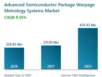
The global advanced semiconductor package warpage metrology systems market size is estimated at USD 229.95 million in 2026 and is projected to reach USD 251.91 million in 2027. Revenue is expected to climb to USD 435.43 million by 2033, growing at a CAGR of 9.55% during 2027-2033. OSATs, foundries, and substrate makers are adding thermal warpage tools because AI accelerator and HBM packages have become so large that bending during solder reflow can decide whether an expensive unit survives assembly.
Packaging houses building chiplet and HBM lines account for much of the new system buying, since each new package construction is usually qualified against JEDEC and IPC warpage requirements before it ships in volume. As per SEMI, assembly and packaging equipment sales are projected to rise 9.6% to USD 6.7 billion in 2026, with advanced and heterogeneous packaging and the performance demands of AI and HBM chips cited among the reasons. That figure covers all back-end tools and does not size warpage metrology, though new packaging lines and package formats are where warpage tool vendors usually find qualification orders.
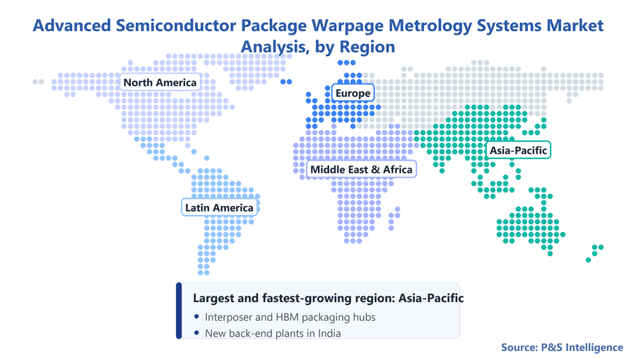
Asia-Pacific accounts for 42% of advanced semiconductor package warpage metrology systems market revenue in 2026 and is projected to post the fastest growth, at a 10.4% CAGR during 2027-2033. Taiwan and South Korea anchor interposer-based AI packaging and HBM stacking, while China and Japan add large OSAT and substrate bases. In the U.S. and Germany, warpage tools more often sit in package development, failure-analysis, and pilot-line laboratories, so purchases there tend to follow research programs and lab upgrades instead of new factory floors.
Key market insights
By technology, optical (non-contact) measurement holds the largest share in 2026.
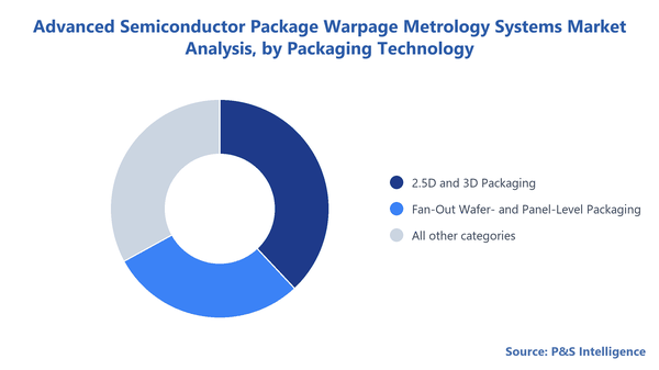
By packaging technology, 2.5D and 3D packaging holds 38% in 2026 and also leads growth, with a projected 10.2% CAGR during 2027-2033.
By end user, OSATs hold 53% in 2026 and are set to expand fastest, at a projected 9.8% CAGR during 2027-2033.
By geography, Asia-Pacific holds 42% in 2026 and is the fastest-growing region, with a projected 10.4% CAGR during 2027-2033.
Advanced Semiconductor Package Warpage Metrology Systems Market Dynamics
In-line warpage checks are reshaping how packaging lines buy metrology
Warpage measurement is starting to move from the reliability lab toward the production floor at advanced packaging sites. Thermal moire and fringe-projection systems still qualify each new design against reflow profiles, but thin dies, large carriers, and tall memory stacks can bend between process steps, and packaging lines gain from shape data captured before a bent part is bonded or molded. This adds a second buying occasion, with production tools bought per line next to the laboratory system bought per package program.
A paper in the Journal of Semiconductor Technology and Science on in-line chip warpage measurement for HBM manufacturing states that wafer and chip warpage become critical quality factors as the number of stacked layers rises, and that no equipment or method yet existed for direct in-line measurement of chip warpage. Memory makers able to measure chip warpage in line could catch bent dies before stacking. Tool vendors that adapt lab methods to production throughput could add a second product line beside the qualification system.
Larger AI and HBM package bodies are driving demand for thermal warpage qualification
AI accelerators that place several logic dies and many HBM stacks on one interposer have pushed package bodies past 100 mm on a side. Uneven thermal expansion between silicon, interposer, and substrate bends large packages during reflow, and a unit that fails coplanarity limits can be scrapped along with every die mounted on it. OSATs and foundries respond by measuring warpage across the full temperature profile for each new package build, which is the purchase case for thermal warpage systems.
A TSMC paper presented at the IEEE Electronic Components and Technology Conference examined CoWoS-R interposers measuring 110 by 110 mm that integrate four SoCs and 12 HBM stacks, describing warpage control as an urgent challenge because it affects joint quality, assembly yield, functional testing, and board-level assembly. Each step up in package size tends to require fresh characterization. Suppliers whose chambers take larger samples and emulate reflow closely are better positioned as such designs approach volume production.
Limited warpage data on glass-core panels is opening demand for large-format thermal tools
Packaging makers moving from round wafers to rectangular panels, and from organic cores to glass, are working with materials whose warpage through reflow has not been characterized in depth. Full-size panels often exceed the field of view of wafer-format tools, so a panel line generally needs metrology sized for the carrier itself. Each pilot line that converts to panels or glass can create demand for large-field thermal systems and for repeated characterization runs while process windows are set.
iNEMI moved the sixth phase of its package warpage prediction and characterization project to panel-level packaging with inorganic materials such as glass substrates or carriers, aiming to measure the dynamic warpage of real samples and build a reliable simulation framework. Consortium work of this kind tends to spread shared measurement methods, which can shorten qualification for later adopters. Vendors able to measure full panels through a reflow profile stand to gain as these lines move from pilot to production.
Method-specific accuracy limits are hindering single-platform purchasing
No single optical method measures every package surface well, which complicates purchasing for buyers that want one platform across many package types. Reflective dies, matte molding compound, and stepped HBM stacks tend to favor different techniques, so laboratories often add measurement heads or send samples to contract labs, and correlating results between methods lengthens evaluations. Smaller OSATs and substrate makers with occasional qualification work may outsource measurement instead of committing capital to a dedicated thermal system.
A review of wafer-level packaging warpage by Arizona State University researchers in Frontiers in Electronics notes that shadow moire heats the sample from one side only, which can leave it unevenly heated, that fringe-projection tools need a calibration step that can affect measurement quality, and that digital image correlation depends on careful sample preparation. Fringe-projection systems with heaters above and below the sample address the first issue. Suppliers that can show correlated results across methods shorten evaluations, while buyers still budget extra time for tool selection.
Segmentation Analysis
Technology
Optical (non-contact) measurement holds the largest share of the advanced semiconductor package warpage metrology systems market in 2026, because qualification requires mapping the whole package surface at each temperature step of a reflow profile, which a point-by-point contact probe is poorly suited to do. Shadow moire tools such as the Akrometrix TherMoire AXP and PS600 series, the fringe-projection Insidix TDM Compact-3, and confocal systems from Takaoka Toko capture full-field shape inside heated chambers, which suits buyers that need complete maps of large substrates and interposers.
Within optical methods, many labs pair techniques, using shadow moire on matte package bodies, fringe projection or confocal on stepped and discontinuous surfaces, and 3D digital image correlation, such as the Akrometrix DIC module, when in-plane strain matters. Laser triangulation profilers such as the Keyence LJ-X series, which check substrate warpage in line, and laser wafer bow and warp tools such as the Kobelco SBW series count here only when sold for package, substrate, interposer, or reconstituted wafer measurement, never for bare-wafer flatness. Multi-method buying favors platforms that add measurement heads to an existing chamber.
Measurement Mode
Thermal (temperature-dependent) warpage systems carry the qualification workload, since JEDEC JESD22-B112 and IPC-9641 define how a package's shape is tracked as it is heated and cooled through a simulated reflow profile. A new package design, substrate supplier, or underfill change usually triggers a fresh thermal run, so these chambers sit with reliability and package-development teams at OSATs, foundries, and substrate makers. Heating uniformity and maximum sample size tend to decide which tool a site buys.
Room-temperature (static) warpage systems handle faster checks on incoming substrates, finished packages, and lot-to-lot screening, where a full reflow simulation adds time without changing the decision. They fit closer to the production line and often become a second purchase once a thermal tool has set the acceptable limits. The two modes tend to be bought by the same lab over time, so vendors that sell both against one analysis software package could win both orders from a single customer.
Packaging Technology
2.5D and 3D packaging holds 38% of revenue in 2026. Interposer-based AI accelerators and stacked memory combine silicon, organic redistribution layers, and molding compound with very different expansion rates on the largest package bodies in production, so each design revision needs full thermal characterization before assembly partners accept it. A single failed unit carries several high-value dies, which raises the cost of a warpage escape and justifies dedicated tool time.
The same category is projected to post the highest CAGR among packaging technologies, at 10.2% during 2027-2033. Taller HBM stacks and more memory stacks per interposer increase the measurement work per package with each product cycle, and hybrid bonding adds steps where bow must stay within tight limits before parts are joined. For OSATs and foundries running these lines, warpage tools can shift from a shared lab asset toward capacity assigned to each customer program.Copyright P&S Intelligence. Reuse requires attribution under CC BY 4.0.
End User
OSATs hold 53% of revenue in 2026, because outsourced assembly houses take on packaging for many chip designers at once and absorb the yield loss when a package warps on their line. They qualify customer designs, materials, and substrate lots against warpage limits for several programs in parallel, which keeps thermal systems busy across shifts. That multi-customer workload tends to justify more than one tool per site and periodic upgrades to larger chambers as package sizes grow.
OSATs are also expected to grow fastest among end users, at a 9.8% CAGR during 2027-2033. Camtek Ltd. said in a March 30, 2026 filing that orders from leading OSATs in the first quarter had already exceeded USD 90 million, mainly for CoWoS-like packaging, and described OSATs as playing an increasingly central role in advanced packaging for AI. Those orders span inspection and metrology broadly, yet they suggest AI packaging work is shifting toward OSATs, which widens the number of sites needing their own warpage capability.
The following segments are analyzed in this report:
Technology
Optical (Non-Contact) Measurement
Others
Measurement Mode
Thermal (Temperature-Dependent) Warpage
Room-Temperature (Static) Warpage
Packaging Technology
2.5D and 3D Packaging (incl. HBM stacks)
Fan-Out Wafer- and Panel-Level Packaging
Others
End User
OSATs
IDMs and Foundries
Research Institutes and Failure-Analysis Laboratories
Regional Analysis
Asia-Pacific advanced semiconductor package warpage metrology systems market outlook
Asia-Pacific holds 42% of the advanced semiconductor package warpage metrology systems market in 2026 and is also projected to grow fastest, at a 10.4% CAGR during 2027-2033. Taiwan hosts much of the interposer-based packaging capacity for AI accelerators, South Korea stacks HBM at its memory makers, and China and Japan add deep OSAT and substrate bases. New package formats are qualified where they are assembled, so a large part of thermal warpage tool shipments goes to these production sites instead of to design centers elsewhere.
Growth in the region increasingly comes from new back-end capacity outside the established hubs. Micron opened its assembly and test facility in Sanand, Gujarat, on February 28, 2026, and expects to assemble and test tens of millions of chips there in 2026, scaling to hundreds of millions in 2027. That site sizes memory assembly volume, not warpage tool demand, though a new back-end plant of this kind typically builds its own reliability and failure-analysis capability, which can include warpage measurement.
Asia-Pacific's lead looks set to widen through 2033, since panel-level lines, glass-core substrates, and taller HBM stacks are likely to reach volume first at packaging houses already operating in the region. India's first installations add to purchases at established sites in Taiwan, South Korea, and Japan. Takaoka Toko in Japan and Koh Young Technology in South Korea sell close to these buyers, while U.S. and European specialists rely partly on distributors and local service partners to compete for the same qualification orders.Copyright P&S Intelligence. Reuse requires attribution under CC BY 4.0.
North America market analysis
North America trails Asia-Pacific in installed volume, with much of its buying concentrated in package development, failure-analysis, and university laboratories. Chip designers and system companies in the U.S. qualify package designs before handing them to assembly partners, so warpage tools there often serve design validation and root-cause work. New domestic packaging plants and research facilities are starting to add production-oriented demand, and Canada contributes through its existing assembly and test base.
According to NIST, the CHIPS National Advanced Packaging Manufacturing Program has finalized USD 300 million in awards for advanced substrate and materials research to Absolics, Applied Materials, and Arizona State University. Research on new substrates depends on characterizing how materials bend under heat, which favors suppliers with large-sample thermal chambers and a U.S. service presence. Purchases tied to such programs follow grant timing, so North American demand is likely to move in steps instead of tracking production volume.
Europe market analysis
Europe holds a smaller, research-led position, with buying concentrated in Germany, France, Italy, and the U.K. among research institutes, automotive and industrial chip makers, and a short list of advanced packaging pilot sites. France is home to Insidix, one of the few specialist thermal warpage vendors, which gives European labs a local supplier and service option. Demand depends more on publicly funded programs and reliability work for automotive electronics than on high-volume AI packaging.
Fraunhofer confirms that the APECS pilot line for advanced packaging and heterogeneous integration started operating in December 2024 under the EU Chips Act, with overall funding of USD 817.81 million (EUR 730 million) over 4.5 years from the Chips Joint Undertaking and national authorities in eight countries, including France and Germany. Pilot lines of this kind typically need warpage data to qualify chiplet assemblies before industrial partners adopt them. Suppliers already serving Fraunhofer institutes and partner laboratories are better positioned for follow-on purchases as chiplet work moves toward production.
Latin America market analysis
Latin America accounts for a small part of global demand, centered on Mexico's electronics manufacturing corridor and Brazil's semiconductor back-end plants. Much of the local packaging work involves memory modules, discrete devices, and mature package types, where room-temperature warpage checks and board-level coplanarity matter more than full thermal characterization of large interposers. Equipment purchases tend to follow new plant investment, which arrives in occasional, project-sized steps.
Brazil's Law No. 14.968, published on September 12, 2024, set up the Brasil Semicon program alongside changes to the PADIS incentive scheme for the semiconductor industry, and a decree issued in July 2026 put the program into operation through 2029. Incentives of this kind support plant upgrades and new packaging lines, which is when reliability labs usually add measurement tools. Buyers in the region tend to source through distributors and regional service partners, so vendors with Latin American channel coverage stand to capture the occasional system order.
Middle East & Africa market analysis
The Middle East & Africa is the smallest contributor, because the region has little high-volume advanced packaging capacity today and commercial demand for package warpage systems is minimal. Saudi Arabia, the U.A.E., and South Africa are the countries where national semiconductor programs and electronics manufacturing could create first tool purchases. Any early orders are likely to be single systems tied to research or new-facility projects.
Saudi Arabia's Research, Development and Innovation Authority announced a National Semiconductor Hub in June 2024 with the objective of supporting 50 specialized companies in electronic chip and semiconductor design. A design-led strategy builds engineering capacity before assembly plants, so package warpage tools are likely to arrive first in research and university laboratories. Suppliers would see larger orders only if the region moves into assembly and test at scale.
The following geographies are analysed in this report.
Asia-Pacific
China
Taiwan
Japan
South Korea
India
Rest of Asia-Pacific
Europe
Germany
France
U.K.
Italy
Rest of Europe
Latin America
Brazil
Mexico
Rest of Latin America
Middle East & Africa
Saudi Arabia
U.A.E.
South Africa
Rest of Middle East & Africa
North America
U.S.
Canada
Advanced Semiconductor Package Warpage Metrology Systems Market Competition Analysis
The advanced semiconductor package warpage metrology systems market splits into two layers with different structures. Dedicated thermal warpage systems, which emulate reflow inside a heated chamber and report shape against JEDEC and IPC limits, come from a short list of specialists, because each tool needs proprietary optics, heating control, and correlation data that customers have accepted in their own qualification files. Once a lab's warpage limits and historical data are built around one vendor's method, switching is costly, so this layer changes slowly.
Akrometrix, Insidix, and Takaoka Toko compete in the dedicated thermal layer, each built around a different optical method, and sell on measurement credibility, chamber size, and the ability to match customers' reflow profiles. KLA, Camtek, Onto Innovation, Nova, and Bruker compete from the wafer and packaging metrology side, where warpage is one measurement within broader process-control platforms sold to foundries, IDMs, and large OSATs. Koh Young Technology and Nordson bring 3D inspection platforms that handle warpage alongside other checks.
The second layer is more open, because platform vendors can add warpage capability to tools that customers already buy for other measurements, and several have done so for advanced packaging lines. Room-temperature checks on incoming substrates and carriers are likely to overlap most with these platforms, since a tool already measuring other features on the line can report bow without a separate heated chamber. A qualification lab and a production line may therefore buy from different vendor groups. Specialists could see some in-line measurement move to platform vendors, while thermal qualification under reflow profiles continues to call for dedicated chambers.
Major Companies in Advanced Semiconductor Package Warpage Metrology Systems Market:
Akrometrix LLC
Insidix SAS
Takaoka Toko Co. Ltd.
KLA Corporation
Camtek Ltd.
Onto Innovation Inc.
Bruker Corporation
Nova Ltd.
Nordson Corporation
Keyence Corporation
Hitachi, Ltd.
Koh Young Technology Inc.
Kobe Steel Ltd.
Advanced Semiconductor Package Warpage Metrology Systems Market News
In July 2026, Nova Ltd. Announced that a leading global foundry selected its Nova WMC platform as tool of record for multiple layers’ measurement in advanced packaging after a competitive evaluation. Nova cited the modular platform’s ability to handle high warpage and non-symmetric shapes in one tool, showing that production packaging metrology increasingly has to cope with warped parts.
In January 2026, Akrometrix LLC released Studio 10.1 software for its warpage systems, adding profile gauges that validate reflow emulation against industry standards, tools that reduce secondary interference effects, and a surface brightness mask. Validated heating profiles help labs show customers that measured warpage matches real reflow conditions.
Last Updated: October 2026
Frequently Asked Questions About This Report
How big is the advanced semiconductor package warpage metrology systems market?+
The global advanced semiconductor package warpage metrology systems market size is estimated at USD 229.95 million in 2026 and is projected to reach USD 251.91 million in 2027.
Why does warpage matter in advanced semiconductor packaging?+
Uneven thermal expansion between silicon, interposer, and substrate bends large packages during reflow, and a unit that fails coplanarity limits can be scrapped along with every die mounted on it.
What are the challenges of package warpage measurement?+
No single optical method measures every package surface well, which complicates purchasing for buyers that want one platform across many package types.
Which standards are used for thermal package warpage measurement?+
Thermal (temperature-dependent) warpage systems carry the qualification workload, since JEDEC JESD22-B112 and IPC-9641 define how a package's shape is tracked as it is heated and cooled through a simulated reflow profile.
Which region leads the package warpage metrology market?+
Asia-Pacific holds 42% of the advanced semiconductor package warpage metrology systems market in 2026 and is also projected to grow fastest, at a 10.4% CAGR during 2027-2033.
Who are the key companies in package warpage measurement systems?+
Akrometrix, Insidix, and Takaoka Toko compete in the dedicated thermal layer, each built around a different optical method, and sell on measurement credibility, chamber size, and the ability to match customers' reflow profiles.
Want a report tailored exactly to your business need?
Leading companies across industries trust us to deliver data-driven insights and innovative solutions for their most critical decisions. From data-driven strategies to actionable insights, we empower the decision-makers who shape industries and define the future. From Fortune 500 companies to innovative startups, we are proud to partner with organisations that drive progress in their industries.
Client Testimonials
Working with P&S Intelligence and their team was an absolute pleasure – their awareness of timelines and commitment to value greatly contributed to our project's success. Eagerly anticipating future collaborations.
McKinsey & Company
India
Unmatched Standards
Our insights into the minutest levels of the markets, including the latest trends and competitive landscape, give you all the answers you need to take your business to new heights
Complete Data Security
We take a cautious approach to protecting your personal and confidential information. Trust is the strongest bond that connects us and our clients, and trust we build by complying with all international and domestic data protection and privacy laws